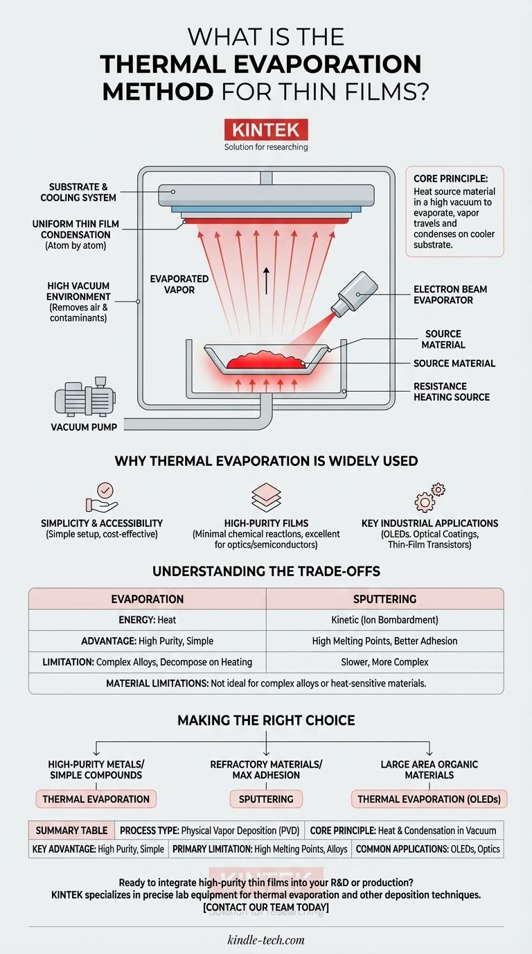
At its core, thermal evaporation is a physical vapor deposition (PVD) method used to create thin films. The process involves heating a source material inside a high-vacuum chamber until it evaporates into a gas. This vapor then travels in a straight line and condenses onto a cooler substrate, building up a uniform, thin layer of the material atom by atom.
The key to understanding thermal evaporation is its elegant simplicity: it leverages basic physics—heating and condensation in a vacuum—to achieve precise control over the creation of incredibly thin, high-purity films essential for modern electronics and optics.
The Mechanics of Thermal Evaporation
To fully grasp the method, it's best to break it down into its fundamental components. The entire process hinges on creating a very specific and controlled environment.
The Critical Role of High Vacuum
The process must occur in a high-vacuum environment. This is non-negotiable for two primary reasons.
First, the vacuum removes air and other gas molecules. This prevents the evaporated source atoms from colliding with anything on their way to the substrate, ensuring a clean, direct path and uniform deposition.
Second, it eliminates contaminants. A vacuum environment prevents unwanted chemical reactions, such as oxidation, ensuring the deposited film is exceptionally pure.
The Heating and Vaporization Stage
To turn the solid source material into a gas, intense heat is required. This is typically achieved in one of two ways.
Resistance heating is the most common method, where a high electrical current is passed through a holder (often called a "boat") containing the source material, causing it to heat up and evaporate.
Alternatively, an electron beam evaporator can be used. This method focuses a high-energy beam of electrons onto the source material, melting and vaporizing it with great precision.
Deposition onto the Substrate
Once the source material becomes a vapor, its atoms or molecules travel through the vacuum chamber.
When this vapor stream hits the cooler surface of the substrate (the object being coated), it rapidly cools and condenses back into a solid state. This condensation process builds the thin film, layer by layer.
Why Thermal Evaporation is Widely Used
Thermal evaporation is a foundational technique in thin-film manufacturing due to its distinct advantages in specific contexts.
Simplicity and Accessibility
Compared to more complex PVD methods like sputtering, thermal evaporation is often simpler in its setup and operation. This can make it a more accessible and cost-effective solution for many applications.
High-Purity Films
Because the process occurs in a high vacuum with minimal chemical reactions, it is excellent for creating films with very high levels of purity. This is critical for semiconductor devices and high-performance optical coatings.
Key Industrial Applications
This method is a cornerstone for producing a range of modern technologies. It is essential for manufacturing Organic Light Emitting Diodes (OLEDs), thin-film transistors, and the precise optical layers on ophthalmic lenses, mirrors, and architectural glass.
Understanding the Trade-offs
No single method is perfect for every scenario. True expertise comes from understanding not just what a tool does, but what it doesn't do well.
Comparison to Sputtering
Thermal evaporation's main counterpart in PVD is sputtering. While evaporation uses heat, sputtering uses kinetic energy, bombarding a target with ions (like argon) to physically knock atoms loose.
Sputtering can deposit materials with extremely high melting points that are difficult to evaporate. It can also produce films with stronger adhesion to the substrate due to the higher energy of the depositing atoms.
Material Limitations
Thermal evaporation is not ideal for all materials. It can be difficult to deposit complex alloys where different elements evaporate at different rates. It is also less effective for materials that decompose when heated.
A Piece of a Larger Puzzle
It's important to remember that thermal evaporation is one of many thin-film techniques. Other methods, such as chemical vapor deposition (CVD), spin coating, and plasma sputtering, are chosen based on the specific material, substrate, and desired film properties.
Making the Right Choice for Your Goal
Selecting a deposition method depends entirely on the material you are working with and the desired outcome for your thin film.
- If your primary focus is creating high-purity films of metals or simple compounds with moderate melting points: Thermal evaporation is often a cost-effective and highly effective choice.
- If your primary focus is depositing refractory materials, complex alloys, or achieving maximum film adhesion and density: A higher-energy process like sputtering is likely the more suitable option.
- If your primary focus is coating large areas with organic materials for flexible electronics: Thermal evaporation is a standard for OLEDs, while solution-based methods like spin coating are used for many polymer compounds.
Understanding the fundamental principles of each deposition technique is the first step toward selecting the optimal method for your specific material and application.
Summary Table:
| Aspect | Key Detail |
|---|---|
| Process Type | Physical Vapor Deposition (PVD) |
| Core Principle | Heating a material in a vacuum until it evaporates and condenses on a substrate. |
| Key Advantage | Produces high-purity films; simple and cost-effective for many materials. |
| Primary Limitation | Less suitable for materials with very high melting points or complex alloys. |
| Common Applications | OLED displays, optical coatings, thin-film transistors. |
Ready to integrate high-purity thin films into your R&D or production? KINTEK specializes in providing the precise lab equipment and consumables you need for thermal evaporation and other deposition techniques. Our experts can help you select the right tools to achieve your specific material and application goals. Contact our team today to discuss your project and discover the KINTEK advantage!
Visual Guide
Related Products
- Molybdenum Tungsten Tantalum Evaporation Boat for High Temperature Applications
- Aluminized Ceramic Evaporation Boat for Thin Film Deposition
- Evaporation Boat for Organic Matter
- Chemical Vapor Deposition CVD Equipment System Chamber Slide PECVD Tube Furnace with Liquid Gasifier PECVD Machine
- Multi Heating Zones CVD Tube Furnace Machine Chemical Vapor Deposition Chamber System Equipment
People Also Ask
- How source material is evaporated during deposition? A Guide to Resistive vs. E-Beam Methods
- What is the difference between thermal evaporation and e beam evaporation? Choose the Right Method for Your Thin Film
- What is thermal evaporation used to deposit? A Guide to Metals, Compounds, and Key Applications
- What are the sources of thermal evaporation? A Guide to Resistive vs. E-Beam Heating
- What is the widely used boat made of in thermal evaporation? Choosing the Right Material for High-Purity Deposition