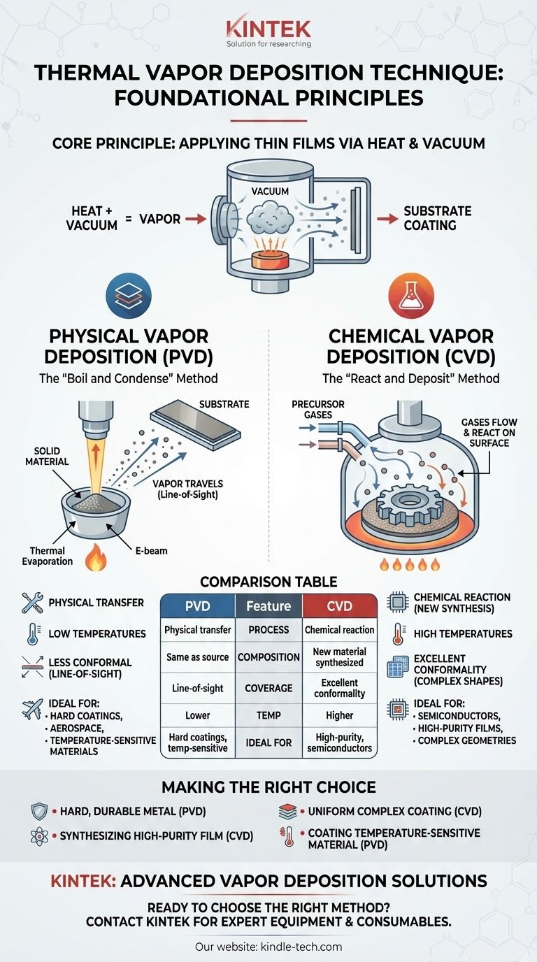
At its core, thermal vapor deposition is not a single technique but a foundational principle used in advanced manufacturing to apply extremely thin films of material onto a surface, known as a substrate. The process universally involves using thermal energy (heat) within a vacuum chamber to turn a source material into a vapor, which then travels and solidifies onto the target substrate, forming a functional coating. This principle is the basis for the two primary methods of vapor deposition: Physical Vapor Deposition (PVD) and Chemical Vapor Deposition (CVD).
The fundamental distinction is simple: Physical Vapor Deposition (PVD) physically transfers an existing material from a source to a substrate, much like steam condensing on a cold window. Chemical Vapor Deposition (CVD) uses precursor gases that undergo a heat-induced chemical reaction on the substrate's surface to create an entirely new solid material as the coating.
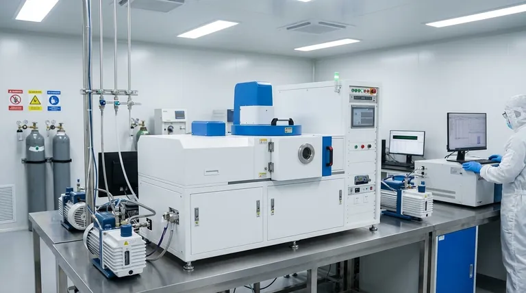
The Fundamentals of a Vapor Deposition System
All thermal vapor deposition processes operate using a similar set of core components designed for precise control over the coating environment. Understanding this setup is key to understanding how these coatings are created.
The Core Components
A typical system consists of three major parts. First is the deposition chamber, which houses the substrate and is sealed to create a vacuum.
Second is the thermal management system. This is critical, as it provides the energy to either vaporize the source material (in PVD) or drive the chemical reaction on the substrate surface (in CVD).
Finally, a controller acts as the brain of the operation. It monitors and adjusts crucial factors like temperature, pressure, and gas flow to ensure the coating is deposited with the desired thickness, purity, and structure.
The Role of Heat and Vacuum
Heat and vacuum are the two non-negotiable elements. Heat supplies the energy needed to transform the source material into a vapor state.
A vacuum is essential for two reasons. It removes air and other particles that could contaminate the coating, and it provides a clear, low-pressure path for the vaporized material to travel from its source to the substrate without unwanted collisions or reactions.
The Two Paths of Thermal Deposition
While both use heat and vacuum, PVD and CVD take fundamentally different approaches to building the coating. The method chosen depends entirely on the material being deposited and the desired properties of the final film.
Physical Vapor Deposition (PVD): The "Boil and Condense" Method
In PVD, a solid or liquid source material is physically converted into a gas. This is often done through methods like heating it until it evaporates (thermal evaporation) or bombarding it with an energy source like an electron beam (e-beam evaporation).
This vapor then travels through the vacuum chamber and condenses directly onto the cooler substrate, forming a solid film. The deposited film has the same chemical composition as the source material.
PVD is widely used for applying dense, temperature-resistant coatings on aerospace components and hard, corrosion-resistant films on cutting tools.
Chemical Vapor Deposition (CVD): The "React and Deposit" Method
CVD begins not with a solid source, but with one or more volatile precursor gases that are injected into the chamber.
The substrate is heated to a specific reaction temperature. When the precursor gases come into contact with the hot surface, they undergo a chemical reaction or decomposition.
The solid product of this reaction is what deposits onto the substrate, building up the film layer by layer. This means the final coating is a new material synthesized directly on the surface. CVD is the standard for creating high-purity semiconductor films, growing carbon nanotubes, and producing photovoltaic layers for solar cells.
Understanding the Trade-offs: PVD vs. CVD
Choosing between PVD and CVD requires understanding their inherent strengths and limitations. The decision is not about which is "better," but which is right for the specific engineering goal.
Material Synthesis vs. Transfer
PVD is excellent for depositing elements and alloys that can be vaporized without decomposing. However, it cannot easily create complex compounds from scratch.
CVD's strength is its ability to synthesize materials, including highly pure crystalline films and complex ceramics, that would be impossible to simply evaporate and deposit.
Conformality and Coverage
Because PVD is a "line-of-sight" process, where vapor travels in a straight line from the source, it can struggle to uniformly coat complex, three-dimensional shapes with deep grooves or hidden surfaces.
CVD, however, uses gases that can flow and diffuse around a complex part before reacting. This often results in a highly conformal coating that covers all exposed surfaces evenly.
Deposition Temperature
PVD processes can often be performed at lower substrate temperatures than CVD. This makes PVD suitable for coating materials that cannot withstand the high heat required to initiate a chemical reaction.
CVD typically requires high temperatures to drive the surface chemistry, which can limit the types of substrates that can be used without being damaged.
Making the Right Choice for Your Application
Your application's specific requirements will dictate the correct technology. Use these guidelines to make an informed decision.
- If your primary focus is applying a hard, durable coating of an existing metal or alloy: PVD is often the more direct and efficient choice for wear resistance and durability.
- If your primary focus is synthesizing a high-purity, crystalline film like silicon or gallium nitride for electronics: CVD is the industry standard due to its unmatched control over film chemistry and structure.
- If your primary focus is uniformly coating a complex, non-flat part: CVD's gas-based process generally provides superior conformality and coverage over intricate geometries.
- If your primary focus is coating a temperature-sensitive plastic or polymer: A lower-temperature PVD process is almost always the necessary choice to avoid damaging the substrate.
Ultimately, understanding the fundamental difference between physically transferring a material and chemically creating one on a surface is the key to mastering vapor deposition.
Summary Table:
| Feature | Physical Vapor Deposition (PVD) | Chemical Vapor Deposition (CVD) |
|---|---|---|
| Process | Physical transfer of vaporized material | Chemical reaction of gases on substrate |
| Coating Composition | Same as source material | New material synthesized on surface |
| Coverage | Line-of-sight; less conformal | Excellent conformality on complex shapes |
| Typical Temperature | Lower temperatures | Higher temperatures required |
| Ideal For | Hard coatings, temperature-sensitive substrates | High-purity films, semiconductors, complex geometries |
Ready to Choose the Right Deposition Method for Your Project?
Understanding the difference between PVD and CVD is crucial for achieving the perfect coating for your components. Whether you need durable tool coatings, high-purity semiconductor films, or conformal layers on complex parts, the right equipment is key to your success.
KINTEK specializes in advanced lab equipment and consumables for all your vapor deposition needs. Our expertise can help you select the ideal system to enhance your research, development, and manufacturing processes.
Contact us today to discuss your specific application and discover how our solutions can bring precision and reliability to your laboratory. Get in touch via our contact form and let's build the future of materials science together.
Visual Guide
Related Products
- HFCVD Machine System Equipment for Drawing Die Nano-Diamond Coating
- Chemical Vapor Deposition CVD Equipment System Chamber Slide PECVD Tube Furnace with Liquid Gasifier PECVD Machine
- Customer Made Versatile CVD Tube Furnace Chemical Vapor Deposition Chamber System Equipment
- Split Chamber CVD Tube Furnace with Vacuum Station Chemical Vapor Deposition System Equipment Machine
- RF PECVD System Radio Frequency Plasma-Enhanced Chemical Vapor Deposition RF PECVD
People Also Ask
- What are the disadvantages and challenges of the HFCVD method? Overcome Growth Limits and Filament Issues
- What types of substrates are used in CVD to facilitate graphene films? Optimize Graphene Growth with the Right Catalyst
- Why is Chemical Vapor Deposition (CVD) equipment uniquely suited for constructing hierarchical superhydrophobic structures?
- What is the hot filament chemical vapour deposition of diamond? A Guide to Synthetic Diamond Coating
- How expensive is chemical vapor deposition? Understanding the True Cost of High-Performance Coating


