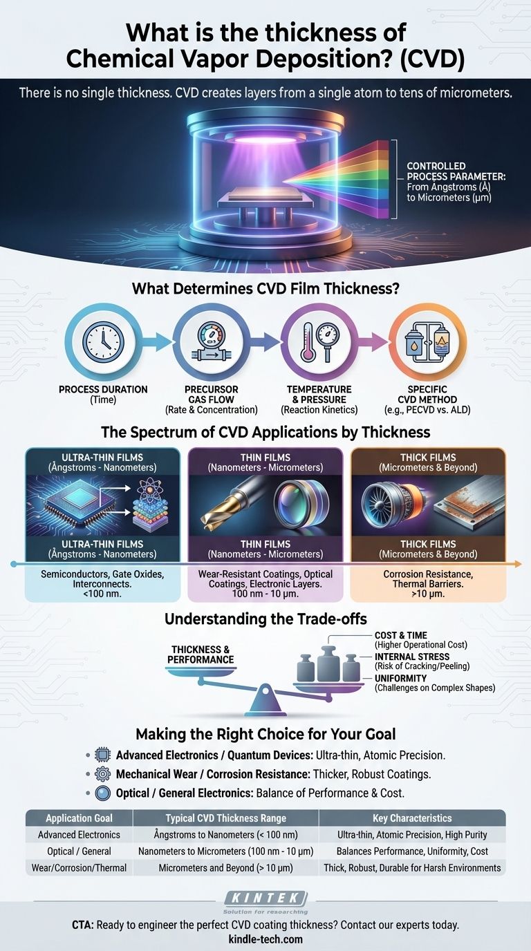
There is no single thickness for chemical vapor deposition (CVD). The thickness of a CVD film is not an inherent property but a highly controlled process parameter, capable of producing layers ranging from a single stratum of atoms (angstroms) to thick protective coatings (tens of micrometers or more). This vast range is precisely why CVD is such a versatile and widely used manufacturing technique.
The core takeaway is that Chemical Vapor Deposition (CVD) is not defined by a specific thickness, but by its exceptional controllability. The final thickness is a deliberate engineering choice determined entirely by the process parameters and the desired application, from nanoelectronics to heavy-duty protective coatings.
What Determines CVD Film Thickness?
The final thickness of a CVD coating is a direct result of several interconnected process variables. Mastering these variables allows for the precise engineering of the film to meet specific performance requirements.
The Role of Process Duration
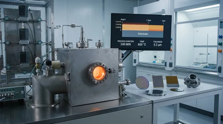
The most straightforward factor is time. In general, allowing the deposition process to run for a longer duration will result in a thicker film as more material is deposited onto the substrate.
Impact of Precursor Gas Flow
The rate and concentration of the precursor gases fed into the reaction chamber directly influence the growth rate. A higher flow of reactive gases generally provides more material for the chemical reaction, leading to a faster deposition and a thicker film in a given amount of time.
The Influence of Temperature and Pressure
Temperature and pressure are critical for controlling the chemical reaction kinetics. Higher temperatures can increase the reaction rate, leading to faster film growth. However, the optimal conditions vary greatly depending on the specific chemicals and desired film properties.
The Specific CVD Method Used
Different types of CVD are optimized for different outcomes. For example, Plasma-Enhanced CVD (PECVD) can achieve high deposition rates at lower temperatures, while a related technique like Atomic Layer Deposition (ALD) builds the film one atomic layer at a time, offering unparalleled precision for ultra-thin films.
The Spectrum of CVD Applications by Thickness
The ability to control thickness across many orders of magnitude allows CVD to be used in an incredibly diverse set of applications.
Ultra-Thin Films (Angstroms to Nanometers)
At the thinnest end of the spectrum, CVD is used to create films that are only a few atoms thick. This level of control is essential in the semiconductor industry for manufacturing the gate oxides and interconnect layers in microchips.
Thin Films (Nanometers to Micrometers)
This is a common range for many industrial applications. Examples include hard, wear-resistant coatings on cutting tools, anti-reflective optical coatings on lenses, and conductive or insulating layers in electronic components.
Thick Films (Micrometers and Beyond)
For applications demanding robust protection, CVD can produce much thicker coatings. These are often used to provide corrosion resistance in harsh chemical environments or to create thermal barriers on components used in high-temperature settings like jet engines.
Understanding the Trade-offs
While CVD is highly versatile, choosing a target thickness involves balancing several practical considerations.
Thickness vs. Cost and Time
The relationship is simple: thicker films take longer to deposit. This directly increases the operational time of expensive equipment and the consumption of precursor gases, leading to a higher cost per part.
Thickness vs. Internal Stress
As a film becomes thicker, internal stress can build up within the material. If not properly managed, this stress can lead to defects such as cracking, peeling, or delamination, causing the coating to fail.
Uniformity Across Complex Shapes
While CVD is a non-line-of-sight process excellent for coating complex surfaces, achieving a perfectly uniform thickness becomes more challenging as the target thickness increases, especially on intricate geometries.
Making the Right Choice for Your Goal
The optimal CVD thickness is dictated entirely by your application's needs.
- If your primary focus is advanced electronics or quantum devices: You will be leveraging CVD's ability to produce highly pure, ultra-thin films with angstrom-level precision.
- If your primary focus is mechanical wear or corrosion resistance: You will require a thicker, more robust coating in the micrometer range to ensure durability.
- If your primary focus is optical or general electronic properties: You will likely work in the range of tens of nanometers to a few micrometers, balancing performance with manufacturing cost.
Ultimately, the thickness of a CVD coating is a powerful design parameter that you control.
Summary Table:
| Application Goal | Typical CVD Thickness Range | Key Characteristics |
|---|---|---|
| Advanced Electronics / Quantum Devices | Ångstroms to Nanometers (< 100 nm) | Ultra-thin, atomic-level precision, high purity |
| Optical Coatings / General Electronics | Nanometers to Micrometers (100 nm - 10 µm) | Balances performance, uniformity, and cost |
| Wear/Corrosion Resistance / Thermal Barriers | Micrometers and Beyond (> 10 µm) | Thick, robust, and durable for harsh environments |
Ready to engineer the perfect CVD coating thickness for your project?
At KINTEK, we specialize in providing the lab equipment and consumables needed to achieve precise, reliable Chemical Vapor Deposition. Whether your research demands atomic-level thin films for semiconductors or durable, thick coatings for industrial components, our solutions are designed to meet your specific laboratory needs.
Contact our experts today to discuss how we can support your CVD process development and help you optimize film thickness for superior results.
Visual Guide
Related Products
- Chemical Vapor Deposition CVD Equipment System Chamber Slide PECVD Tube Furnace with Liquid Gasifier PECVD Machine
- RF PECVD System Radio Frequency Plasma-Enhanced Chemical Vapor Deposition RF PECVD
- Microwave Plasma Chemical Vapor Deposition MPCVD Machine System Reactor for Lab and Diamond Growth
- Customer Made Versatile CVD Tube Furnace Chemical Vapor Deposition Chamber System Equipment
- 915MHz MPCVD Diamond Machine Microwave Plasma Chemical Vapor Deposition System Reactor
People Also Ask
- How are carbon nanotubes grown? Master Scalable Production with Chemical Vapor Deposition
- What are the advantages of chemical vapor deposition? Achieve Superior Thin Films for Your Lab
- Why is Chemical Vapor Deposition (CVD) equipment uniquely suited for constructing hierarchical superhydrophobic structures?
- What types of substrates are used in CVD to facilitate graphene films? Optimize Graphene Growth with the Right Catalyst
- What are the core advantages of PE-CVD in OLED encapsulation? Protect Sensitive Layers with Low-Temp Film Deposition


