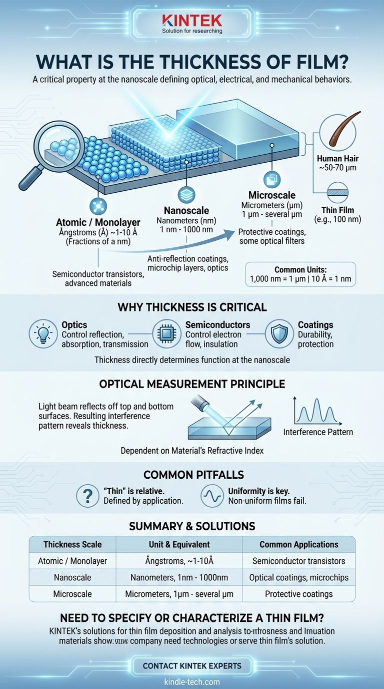
In the simplest terms, a thin film is a layer of material with a thickness ranging from a single layer of atoms (fractions of a nanometer) up to several micrometers. The most common unit of measurement is the nanometer (nm), but values are also frequently expressed in angstroms (Å) or micrometers (µm).
The critical takeaway is that a film's thickness is not just a dimension; it is the primary property that defines its function. At this microscopic scale, thickness directly controls a material's optical, electrical, and mechanical behaviors.
Defining the Scale of "Thin Film"
Understanding the term "thin film" requires grasping the incredibly small scales involved. This isn't like a coat of paint; it's a precisely engineered layer often invisible to the naked eye.
From Atoms to Microns
A thin film can be as thin as a monolayer, which is a single, tightly packed layer of atoms. This is the absolute thinnest a film can be.
The upper limit is typically considered to be several micrometers (also called microns). For perspective, a single human hair is about 50 to 70 micrometers thick, making most thin films dozens or even hundreds of times thinner.
Common Units of Measurement
You will encounter three primary units when discussing film thickness:
- Micrometer (µm): One-millionth of a meter.
- Nanometer (nm): One-billionth of a meter (1,000 nm = 1 µm).
- Angstrom (Å): One ten-billionth of a meter (10 Å = 1 nm).
Most discussions in optics and semiconductors happen at the nanometer scale.
Why Thickness is the Critical Property
For thin films, thickness is the most important design parameter. The entire purpose of creating such a layer is to leverage the unique properties that emerge only at these specific dimensions.
How Thickness Determines Function
A material's behavior changes at the nanoscale. The thickness of a film is precisely controlled to achieve a specific outcome, such as manipulating light for an anti-reflection coating on eyeglasses or controlling electron flow in a microchip.
The Principle of Optical Measurement
Thickness is often measured by analyzing light. A beam of light is directed at the film, and it reflects off both the top surface and the bottom surface of the film.
These two reflected light waves interfere with each other. By analyzing the resulting interference pattern (the peaks and valleys in the light spectrum), engineers can calculate the film's thickness with extreme precision.
The Role of Material Type
This measurement process is entirely dependent on the film's refractive index, a property that describes how light travels through that specific material. Therefore, you cannot measure thickness without also knowing the material the film is made of.
Common Pitfalls to Avoid
While the concept seems straightforward, the practical application has important nuances that are crucial to understand.
"Thin" is a Relative Term
There is no universal standard for what constitutes a "thin film" versus a "coating" or "layer." The term's meaning is always defined by the specific application and the functional properties being targeted.
Uniformity is as Important as Thickness
A single thickness value is an ideal. In practice, a key challenge is uniformity—ensuring the film has the exact same thickness across the entire surface. A non-uniform film will fail to perform its intended function correctly.
Making the Right Choice for Your Goal
The "correct" thickness is determined entirely by the intended application.
- If your primary focus is optics (e.g., lenses, solar panels): Thickness is engineered to fractions of a wavelength of light to control reflection, absorption, or transmission.
- If your primary focus is semiconductors (e.g., microchips): Thickness is controlled at the atomic level to create the insulating and conductive layers that form transistors.
- If your primary focus is protective coatings (e.g., tools, medical devices): Thickness is a balance between providing durability and not altering the underlying part's dimensions or function.
Ultimately, a film's thickness should be seen as a deliberate design choice that unlocks the material's desired properties.
Summary Table:
| Thickness Scale | Unit | Equivalent | Common Applications |
|---|---|---|---|
| Atomic / Monolayer | Ångstroms (Å) | ~1-10 Å | Semiconductor transistors, advanced materials |
| Nanoscale | Nanometers (nm) | 1 nm - 1000 nm | Anti-reflection coatings, microchip layers, optics |
| Microscale | Micrometers (µm) | 1 µm - several µm | Protective coatings, some optical filters |
Need to Specify or Characterize a Thin Film for Your Project?
The precise thickness of your film is not just a number—it's the foundation of its performance. Whether you are developing optical coatings, semiconductor devices, or protective layers, achieving the correct and uniform thickness is critical.
KINTEK specializes in the equipment and consumables needed for precise thin film deposition and analysis. Our solutions help researchers and engineers in laboratories control this vital parameter to ensure their materials function as designed.
Contact our experts today to discuss your specific application. We can help you select the right tools to achieve the exact film thickness your project requires for success.
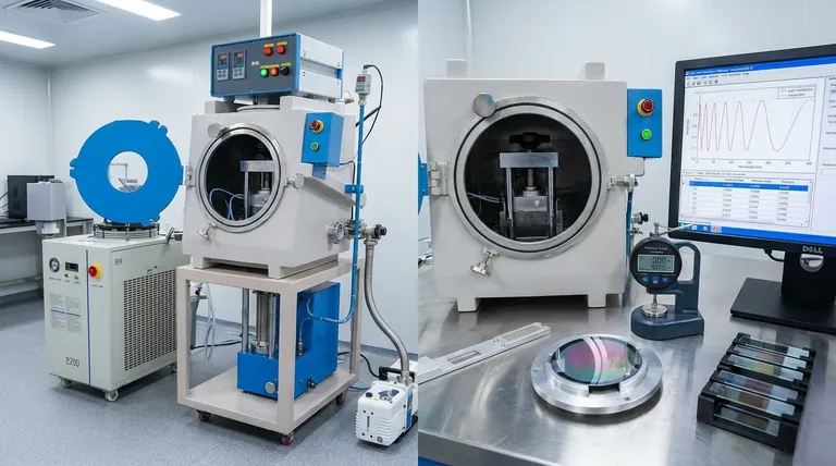
Visual Guide
Related Products
- Aluminized Ceramic Evaporation Boat for Thin Film Deposition
- Tungsten Evaporation Boat for Thin Film Deposition
- Electron Beam Evaporation Coating Oxygen-Free Copper Crucible and Evaporation Boat
- Molybdenum Tungsten Tantalum Evaporation Boat for High Temperature Applications
- Aluminum-Plastic Flexible Packaging Film for Lithium Battery Packaging
People Also Ask
- What are thin films deposited by evaporation? A Guide to High-Purity Coating
- What are the alternatives to sputtering? Choose the Right Thin Film Deposition Method
- What is thin film deposition? Unlock Advanced Surface Engineering for Your Materials
- What is the chemical method for thin film deposition? Build Films from the Molecular Level Up
- Why is an alumina boat and Ti3AlC2 powder bed necessary for Ti2AlC sintering? Protect MAX Phase Purity


