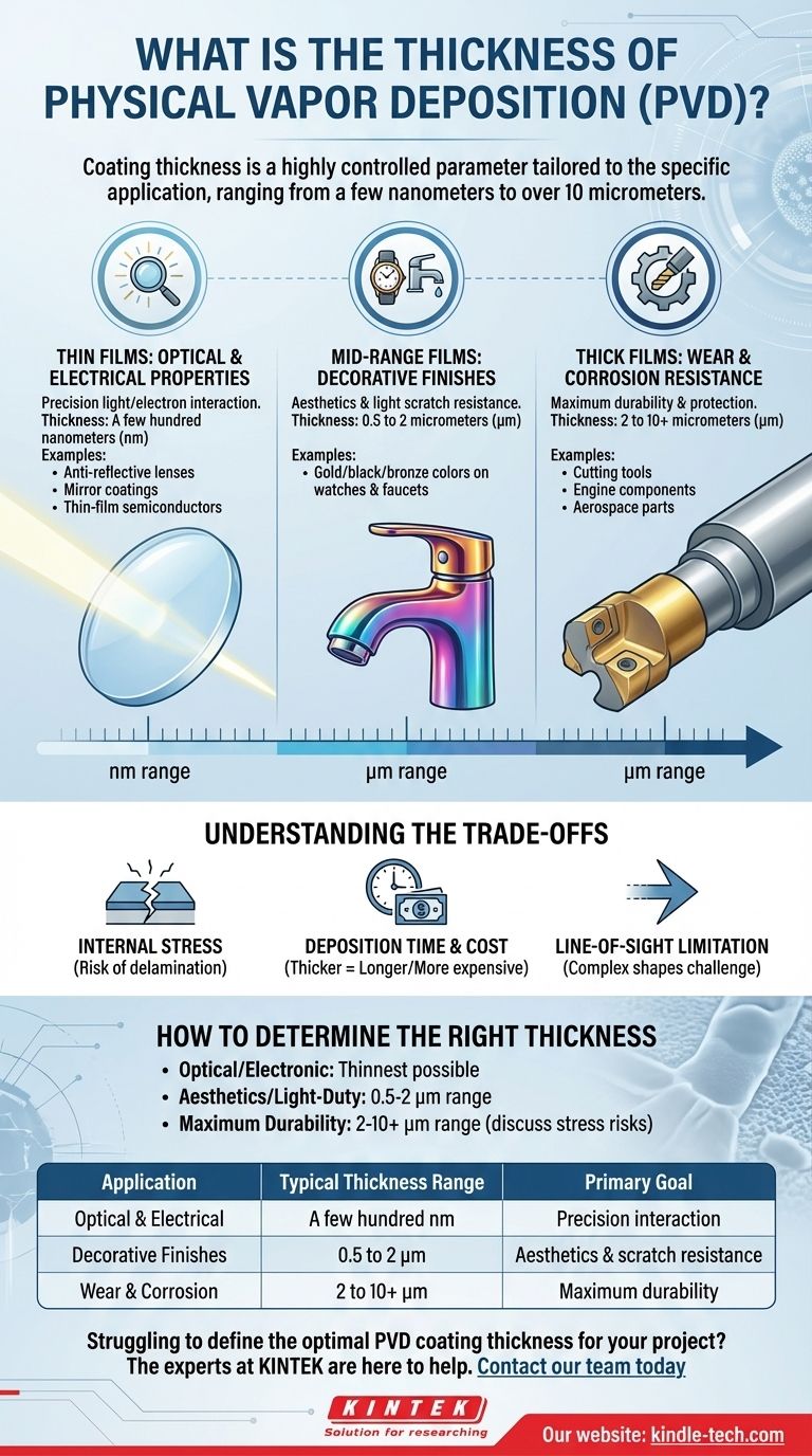
In physical vapor deposition (PVD), there is no single standard thickness. Coating thickness is a highly controlled parameter that is tailored to the specific application, typically ranging from a few nanometers for optical films to over 10 micrometers for heavy-duty wear-resistant layers.
The critical insight is not to ask "what is the thickness," but rather "what thickness is required for my specific goal?" PVD thickness is a direct function of the desired outcome, whether that is manipulating light, providing color, or creating a durable barrier against wear.
Why PVD Thickness Varies: A Matter of Function
The required thickness of a PVD coating is dictated entirely by the problem it is designed to solve. Different applications demand vastly different film properties, which are directly tied to how thick the material is deposited.
Thin Films for Optical & Electrical Properties
For applications like anti-reflective coatings on lenses, mirror coatings, or thin-film semiconductors, precision is paramount. These coatings are often just a few hundred nanometers (nm) thick.
Their function relies on interacting with wavelengths of light or controlling the flow of electrons over microscopic distances. Any unnecessary thickness would disrupt this performance, so films are kept as thin as functionally possible.
Mid-Range Films for Decorative Finishes
When PVD is used for decorative purposes, such as adding a gold, black, or bronze color to a watch or faucet, the primary goals are appearance and light scratch resistance.
These coatings typically fall in the 0.5 to 2 micrometer (µm) range. This is thick enough to provide a durable, uniform color but not so thick that it becomes cost-prohibitive or introduces significant stress.
Thick Films for Wear & Corrosion Resistance
For industrial applications, such as coating cutting tools, engine components, or aerospace parts, the goal is maximum durability. These are known as tribological (wear-resistant) or hard coatings.
These layers are significantly thicker, often ranging from 2 to 10 µm, and can sometimes exceed this. The added material acts as a sacrificial barrier, protecting the underlying component from abrasion, friction, heat, and chemical attack.
Understanding the Trade-offs of PVD Thickness
Simply depositing a thicker coating is not always better. The process involves critical trade-offs that must be balanced for a successful application.
The Problem of Internal Stress
As a PVD coating gets thicker, internal stress builds within the deposited material. If this stress becomes too high, it can cause the coating to become brittle, crack, or even peel away from the substrate—a failure known as delamination.
Deposition Time and Cost
PVD is a batch process that occurs within a vacuum chamber. The deposition rate is relatively slow, meaning thicker coatings require significantly longer cycle times. This directly translates to higher energy consumption and a more expensive final part.
The Line-of-Sight Limitation
PVD is a line-of-sight process, meaning the coating material travels in a straight line from the source to the target part. Achieving a uniform thick coating on a complex, three-dimensional shape is challenging and may require sophisticated part rotation and multiple coating sources.
How to Determine the Right Thickness for Your Application
Use your end goal to guide your technical specification. Partnering with a PVD expert is always recommended, but these principles will help you define your requirements.
- If your primary focus is optical or electronic performance: Specify the thinnest possible film that achieves the desired effect, often measured in nanometers.
- If your primary focus is aesthetics and light-duty protection: A moderate thickness in the 0.5 to 2-micrometer range is a robust and cost-effective target.
- If your primary focus is maximum durability and wear resistance: A thicker coating from 2 to 10 micrometers is necessary, but you must discuss the risk of internal stress with your coating provider.
Ultimately, selecting the right PVD thickness is a strategic engineering decision that balances performance requirements with the inherent limitations of the process.
Summary Table:
| Application | Typical Thickness Range | Primary Goal |
|---|---|---|
| Optical & Electrical | A few hundred nanometers (nm) | Precision light/electron interaction |
| Decorative Finishes | 0.5 to 2 micrometers (µm) | Aesthetics & light scratch resistance |
| Wear & Corrosion Resistance | 2 to 10+ micrometers (µm) | Maximum durability & protection |
Struggling to define the optimal PVD coating thickness for your project? The experts at KINTEK are here to help. We specialize in providing tailored lab equipment and consumables for precise PVD applications, ensuring your coatings deliver the exact performance you need—whether for optical clarity, decorative appeal, or industrial durability. Contact our team today to discuss your specific requirements and achieve superior results with the right coating solution.
Visual Guide
Related Products
- Custom CVD Diamond Coating for Lab Applications
- HFCVD Machine System Equipment for Drawing Die Nano-Diamond Coating
- CVD Diamond for Thermal Management Applications
- Electron Beam Evaporation Coating Oxygen-Free Copper Crucible and Evaporation Boat
- RF PECVD System Radio Frequency Plasma-Enhanced Chemical Vapor Deposition RF PECVD
People Also Ask
- What are the types of CVD coating? A Guide to Choosing the Right Process
- What is CVD diamond coating? Grow a Super-Hard, High-Performance Diamond Layer
- What is the use of CVD coating? Enhance Durability and Functionality for Your Components
- What are the advantages of CVD coating? Superior Hardness and Uniformity for Demanding Applications
- How thick is CVD diamond coating? Balancing Durability and Stress for Optimal Performance


