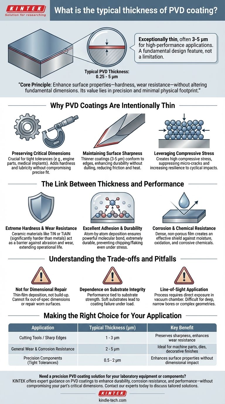
In practice, the typical thickness of a PVD coating is exceptionally thin, generally ranging from 0.25 to 5 microns (µm). For many high-performance applications, such as cutting tools, the coating is often kept between 3 and 5 microns. This microscopic thickness is not a limitation but a fundamental design feature of the technology.
The core principle of Physical Vapor Deposition (PVD) is to enhance a component's surface properties—like hardness and wear resistance—without altering its fundamental dimensions, sharpness, or mechanical integrity. Its value lies in its precision and minimal physical footprint.
Why PVD Coatings Are Intentionally Thin
The microscopic thickness of PVD coatings is a primary reason for their adoption in precision engineering. It allows for surface enhancement on a molecular level while preserving the part's original design intent.
Preserving Critical Dimensions
For components with tight tolerances, such as engine parts, medical implants, or precision molds, any significant change in dimension can lead to failure.
A coating of just a few microns adds extreme surface hardness and lubricity without compromising the precise fit and function of the component.
Maintaining Surface Sharpness
The references note that thinner coatings are crucial for cutting tools. This is because a thick coating would round a sharp cutting edge, increasing friction and heat while reducing cutting efficiency.
A PVD layer of 3 to 5 microns is thin enough to conform perfectly to a sharpened edge, enhancing its durability without dulling it. This results in longer tool life and cleaner cuts.
Leveraging Compressive Stress
The PVD process creates a layer with high compressive stress. This means the coating molecules are tightly packed, effectively pushing against each other.
This internal stress helps to suppress the formation and growth of micro-cracks on the surface, making the component more resilient to the cyclical impacts found in processes like milling.
The Link Between Thickness and Performance
Even at a thickness of a few microns, a PVD coating dramatically alters the functional surface of a component. The performance gains are a direct result of the material being deposited and the strong bond it forms.
Extreme Hardness and Wear Resistance
PVD coatings are often ceramic materials like Titanium Nitride (TiN) or Titanium Aluminum Nitride (TiAlN), which are significantly harder than most metals.
This thin, hard layer acts as a barrier, protecting the underlying substrate from abrasion, friction, and wear, thereby extending the component's operational life.
Excellent Adhesion and Durability
The coating is deposited in a vacuum chamber, atom by atom, ensuring a powerful molecular bond with the substrate.
Unlike plating, which can chip or flake, a properly applied PVD coating is extremely durable and stays bonded even under significant stress and thermal cycling. The relatively low application temperatures (250°C - 750°C) also prevent thermal damage or distortion of the base material.
Corrosion and Chemical Resistance
The deposited film is dense and non-porous, creating an effective shield against moisture, oxidation, and many corrosive chemicals. This is a key benefit for components used in harsh environments.
Understanding the Trade-offs and Pitfalls
While highly effective, PVD coatings have specific limitations that are critical to understand for successful application.
Not for Dimensional Repair
PVD is a thin-film deposition process, not a build-up process. It cannot be used to fix out-of-spec dimensions, fill in scratches, or repair worn surfaces. The substrate must be in its final, finished state before coating.
Dependence on Substrate Integrity
The performance of the coating is fundamentally tied to the strength of the material underneath it. Applying a very hard PVD coating to a soft substrate will not prevent failure under heavy load.
If the base material deforms, the thin ceramic coating will crack and fail. The substrate must provide the foundational strength.
Line-of-Sight Application
The PVD process works on a line-of-sight basis. This means surfaces must be directly exposed to the source material inside the vacuum chamber to be coated.
Deep, narrow bores or complex internal geometries can be very difficult or impossible to coat evenly, which is a key consideration during the design phase.
Making the Right Choice for Your Application
The ideal coating thickness is determined entirely by the component's function and operational demands.
- If your primary focus is cutting tools or sharp edges: Opt for a thinner coating (1-3 µm) to preserve the blade's sharpness while gaining significant wear resistance.
- If your primary focus is general wear and corrosion resistance: A standard thickness (2-5 µm) is typically ideal for machine parts, dies, and decorative finishes where ultimate sharpness is not the main concern.
- If your primary focus is precision components with tight tolerances: Use the thinnest effective coating possible (0.5-2 µm) to enhance surface properties without impacting the part's critical dimensions.
Ultimately, PVD technology delivers its greatest value by adding immense surface durability with almost no dimensional change.
Summary Table:
| Application | Typical Thickness (µm) | Key Benefit |
|---|---|---|
| Cutting Tools / Sharp Edges | 1 - 3 µm | Preserves sharpness, enhances wear resistance |
| General Wear & Corrosion Resistance | 2 - 5 µm | Ideal for machine parts, dies, and decorative finishes |
| Precision Components (Tight Tolerances) | 0.5 - 2 µm | Enhances surface properties without dimensional impact |
Need a precision PVD coating solution for your laboratory equipment or components? KINTEK specializes in high-performance lab equipment and consumables, offering expert guidance on PVD coatings to enhance durability, corrosion resistance, and performance—without compromising your part's critical dimensions. Contact our experts today to discuss how our tailored PVD solutions can extend the life and reliability of your laboratory tools and components.
Visual Guide
Related Products
- RF PECVD System Radio Frequency Plasma-Enhanced Chemical Vapor Deposition RF PECVD
- Custom CVD Diamond Coating for Lab Applications
- Vacuum Hot Press Furnace Machine for Lamination and Heating
- Vacuum Cold Trap Direct Cold Trap Chiller
- Isostatic Molding Pressing Molds for Lab
People Also Ask
- Why does PECVD commonly use RF power input? For Precise Low-Temperature Thin Film Deposition
- Why is PECVD environment friendly? Understanding the Eco-Friendly Benefits of Plasma-Enhanced Coating
- What are the advantages of PECVD? Enable Low-Temperature, High-Quality Thin-Film Deposition
- What are the applications of PECVD? Essential for Semiconductors, MEMS, and Solar Cells
- What are the benefits of PECVD? Achieve Superior Low-Temperature Thin Film Deposition