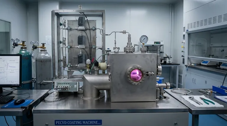
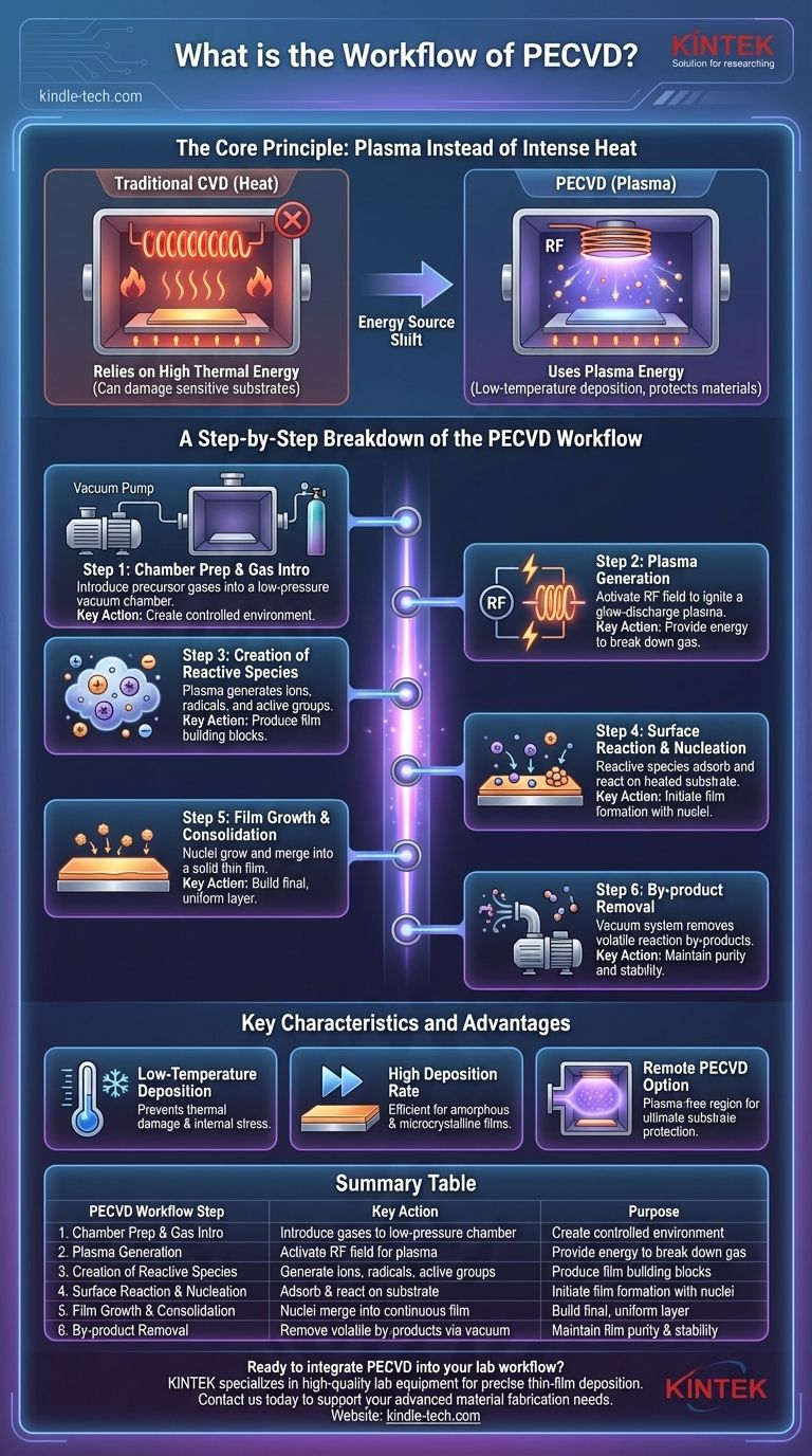
At its core, Plasma-Enhanced Chemical Vapor Deposition (PECVD) is a process that uses the energy of a plasma to deposit a high-quality thin film onto a substrate. The workflow begins by introducing precursor gases into a low-pressure chamber, where a radio frequency (RF) field ignites the gas into a plasma. This energetic plasma breaks the gas molecules into reactive chemical species that then land on the substrate surface, react, and build up layer by layer to form the final film.
The critical takeaway is that PECVD replaces the intense heat required by traditional deposition methods with the energy of a plasma. This fundamental shift allows for film deposition at significantly lower temperatures, making it possible to coat sensitive materials that would otherwise be damaged by heat.
The Core Principle: Plasma Instead of Intense Heat
To understand the PECVD workflow, you must first grasp the problem it solves. The key is its relationship to traditional Chemical Vapor Deposition (CVD).
The Limitation of Traditional CVD
Traditional CVD relies exclusively on thermal energy. A substrate is heated to very high temperatures, which provides the energy needed to break down precursor gases and drive the chemical reactions that form the film.
This high-heat requirement is a significant constraint, as it can damage temperature-sensitive substrates like electronic components or plastics.
The PECVD Advantage: Energy from Plasma
PECVD bypasses the need for extreme heat by creating a plasma. The process still uses a heated substrate, but at a much lower temperature.
An RF electric field energizes the precursor gases, stripping electrons and creating a mix of ions, electrons, and highly reactive neutral species. These energetic particles have enough energy (typically 1-10 eV) to break chemical bonds and drive reactions without high thermal input.
A Step-by-Step Breakdown of the PECVD Workflow
The PECVD process can be broken down into a series of well-defined steps, all occurring within a controlled vacuum chamber.
Step 1: Chamber Preparation and Gas Introduction
First, a substrate is placed inside the reaction chamber, which is then pumped down to a low-pressure environment (typically 50 mtorr to 5 torr).
Once the vacuum is stable, precisely controlled amounts of one or more precursor gases are introduced into the chamber.
Step 2: Plasma Generation
An RF power source (usually between 100 kHz and 40 MHz) is activated. This creates a strong electric field within the chamber.
The field energizes the precursor gas, causing it to break down and form a glow-discharge plasma.
Step 3: Creation of Reactive Species
Within the plasma, collisions between energetic electrons and gas molecules create a soup of ions, radicals, and other active groups. These are the highly reactive building blocks for the film.
Step 4: Surface Reaction and Nucleation
These reactive species diffuse through the chamber and adsorb onto the surface of the heated substrate.
On the surface, they undergo chemical reactions to form the desired material. This process begins with the formation of tiny, stable clusters known as crystal nuclei.
Step 5: Film Growth and Consolidation
These nuclei act as seeds, growing and merging into larger, island-like structures.
Eventually, the islands coalesce to form a continuous, solid thin film across the entire substrate surface.
Step 6: By-product Removal
The chemical reactions also create unwanted by-products. These volatile compounds detach from the surface and are continuously removed from the chamber by the vacuum pump system.
Key Characteristics and Considerations
The unique workflow of PECVD results in several distinct advantages and characteristics that differentiate it from other methods.
The Primary Benefit: Low-Temperature Deposition
The ability to deposit films at low temperatures is PECVD's defining feature. This prevents thermal damage and reduces internal stress caused by a mismatch in thermal expansion between the film and the substrate.
Another Advantage: High Deposition Rate
PECVD can achieve relatively high deposition rates, which is especially beneficial for producing amorphous and microcrystalline films used in solar cells and thin-film transistors.
A Critical Variation: Remote PECVD
In some cases, the plasma itself can still cause damage to a highly sensitive substrate. The Remote PECVD method solves this.
In this variation, the plasma is generated in a separate chamber. Only the desired reactive species are extracted and transported to the substrate, which remains in a plasma-free region, offering maximum protection.
Making the Right Choice for Your Goal
Understanding the PECVD workflow empowers you to decide if it's the correct tool for your specific application.
- If your primary focus is coating temperature-sensitive materials: PECVD is the ideal choice, as its low-temperature process prevents damage to electronics, polymers, and other delicate substrates.
- If your primary focus is minimizing film stress: PECVD's low-temperature nature significantly reduces the thermal stress that can cause films to crack or delaminate.
- If your primary focus is achieving high throughput for amorphous films: The high deposition rates of PECVD make it an efficient manufacturing technique for components like solar panels.
- If your primary focus is ultimate substrate protection: Consider Remote PECVD to shield your material from any direct interaction with the plasma environment.
By substituting plasma energy for extreme heat, PECVD unlocks new possibilities for advanced material fabrication.
Summary Table:
| PECVD Workflow Step | Key Action | Purpose |
|---|---|---|
| 1. Chamber Prep & Gas Intro | Introduce precursor gases into a low-pressure chamber. | Create a controlled environment for the reaction. |
| 2. Plasma Generation | Activate an RF field to ignite a glow-discharge plasma. | Provide energy to break down gas molecules. |
| 3. Creation of Reactive Species | Plasma generates ions, radicals, and active groups. | Produce the building blocks for the thin film. |
| 4. Surface Reaction & Nucleation | Reactive species adsorb and react on the heated substrate. | Initiate film formation with crystal nuclei. |
| 5. Film Growth & Consolidation | Nuclei grow and merge into a continuous thin film. | Build the final, uniform film layer by layer. |
| 6. By-product Removal | Vacuum system removes volatile reaction by-products. | Maintain film purity and process stability. |
Ready to integrate PECVD into your lab workflow? KINTEK specializes in high-quality lab equipment and consumables for precise thin-film deposition. Our expertise ensures you get the right PECVD solutions for coating temperature-sensitive substrates like electronics and polymers, minimizing stress and maximizing throughput. Contact us today to discuss how we can support your laboratory's advanced material fabrication needs. Get in touch with our experts now!
Visual Guide
Related Products
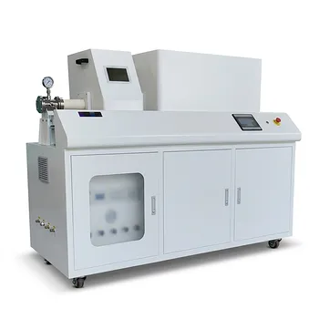
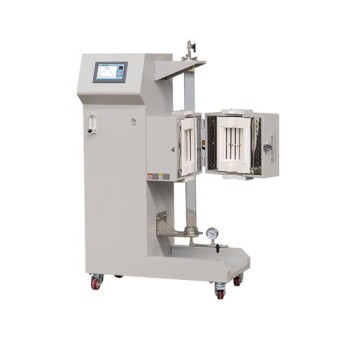
- Inclined Rotary Plasma Enhanced Chemical Vapor Deposition PECVD Equipment Tube Furnace Machine
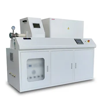
- Chemical Vapor Deposition CVD Equipment System Chamber Slide PECVD Tube Furnace with Liquid Gasifier PECVD Machine
- Inclined Rotary Plasma Enhanced Chemical Vapor Deposition PECVD Equipment Tube Furnace Machine
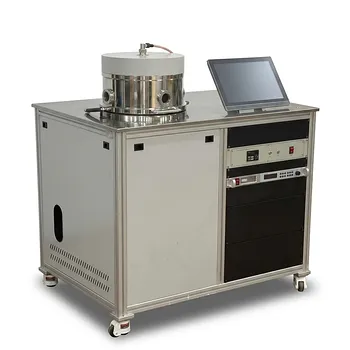
- RF PECVD System Radio Frequency Plasma-Enhanced Chemical Vapor Deposition RF PECVD
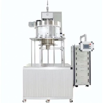
- Multi Heating Zones CVD Tube Furnace Machine Chemical Vapor Deposition Chamber System Equipment
People Also Ask
- How does PECVD equipment facilitate the directional growth of carbon nanotubes? Achieve Precision Vertical Alignment
- How does plasma enhanced chemical vapor deposition work? Enable Low-Temperature Thin Film Deposition
- What is the process of PECVD in semiconductor? Enabling Low-Temperature Thin Film Deposition
- How does PECVD process work? Achieve Low-Temperature, High-Quality Thin Films
- What are the advantages of plasma enhanced chemical vapor deposition? Enable Low-Temperature, High-Quality Film Deposition
