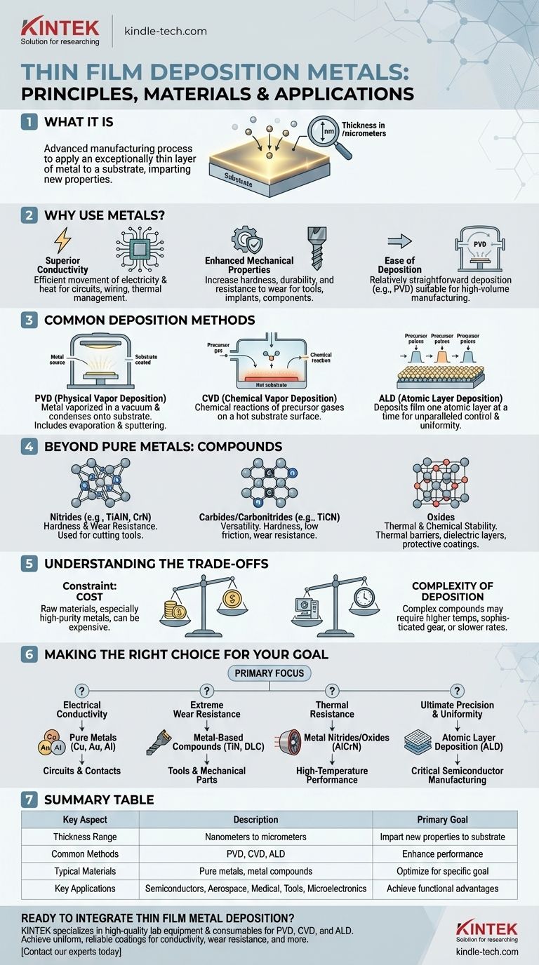
In essence, thin film metal deposition is an advanced manufacturing process where an exceptionally thin layer of metal, often just nanometers to micrometers thick, is applied to a substrate's surface. This is done to impart new properties to the substrate, such as electrical conductivity, durability, or corrosion resistance, that it did not originally possess. Metals are frequently chosen for their excellent conductive properties, strength, and relative ease of application.
The core principle is not just to coat a surface, but to fundamentally alter its function. Metals are a foundational choice for this process due to their inherent electrical, thermal, and mechanical strengths, but the true engineering lies in selecting the right metal or metal compound and deposition method for a specific goal.
Why Use Metals for Thin Film Deposition?
The decision to use metals in thin film applications is driven by their unique and powerful physical properties. These characteristics make them indispensable in industries ranging from semiconductors to aerospace.
Superior Conductivity
Metals are the premier choice for applications requiring efficient movement of electricity or heat. This makes them essential for creating the conductive pathways in integrated circuits, wiring in microelectronics, and reflective coatings for thermal management.
Enhanced Mechanical Properties
Depositing a thin film of metal or a metal compound can dramatically increase a substrate's surface hardness, durability, and resistance to wear and tear. This is a common strategy for extending the life of cutting tools, medical implants, and machine components.
Ease of Deposition
Compared to more complex compounds, many pure metals are relatively straightforward to deposit onto a substrate. Techniques like Physical Vapor Deposition (PVD) can efficiently apply metal films, making them suitable for high-volume manufacturing.
Common Deposition Methods Explained
The method used to apply the thin film is just as critical as the material itself. The choice of technique directly influences the film's quality, purity, and cost.
Physical Vapor Deposition (PVD)
PVD is a widely used technique for metals. It involves a process where the source metal is vaporized in a vacuum—either by heating it (evaporation) or bombarding it with ions (sputtering)—and then allowed to condense onto the substrate, forming a thin, uniform film.
Chemical Vapor Deposition (CVD)
CVD uses chemical reactions to form the film. Precursor gases containing the desired metal are introduced into a chamber, where they react or decompose on the hot substrate surface, leaving behind a high-purity, often very hard, thin film.
Atomic Layer Deposition (ALD)
For applications demanding the utmost precision, ALD deposits the film one single atomic layer at a time. This process offers unparalleled control over thickness and uniformity, which is critical for advanced semiconductor manufacturing.
Beyond Pure Metals: The Role of Compounds
While pure metals are foundational, many of the most advanced coatings are actually metal-based compounds, where metals are combined with other elements to achieve highly specific properties.
Nitrides for Hardness and Wear Resistance
Metal nitrides, such as Titanium Aluminum Nitride (Ti-Al-N) and Chromium Nitride (Cr-N), are exceptionally hard and corrosion-resistant. They are frequently used as coatings on industrial cutting tools to increase their lifespan and performance.
Carbides and Carbonitrides for Versatility
Adding carbon creates compounds like Titanium Carbonitride (Ti-C-N), which offers a unique balance of hardness, low friction, and wear resistance, making it a versatile solution for many mechanical applications.
Oxides for Thermal and Chemical Stability
Metal oxides are highly valued for their toughness and ability to withstand high temperatures. They serve as thermal barriers, dielectric layers in capacitors, and protective coatings in harsh chemical environments.
Understanding the Trade-offs
Selecting a material and process is never without compromises. Acknowledging these limitations is key to making an informed engineering decision.
The Primary Constraint: Cost
A significant drawback of using certain metals and metal compounds is their expense. The cost of raw materials, especially for high-purity metals, can limit their use in certain price-sensitive applications.
Complexity of Deposition
While some metals are easy to deposit, working with complex compounds can be challenging. These materials may require higher temperatures, more sophisticated equipment, or slower deposition rates, which adds to the overall cost and complexity of manufacturing.
Technique vs. Material
Sometimes the desired film property, such as extreme purity or perfect uniformity, is dictated more by the deposition technique (e.g., ALD) than the material itself. The most advanced techniques are often the slowest and most expensive.
Making the Right Choice for Your Goal
Your final decision should be guided by the primary objective you need to achieve.
- If your primary focus is electrical conductivity: Pure metals like copper, gold, or aluminum are the most direct and effective choice for creating circuits and contacts.
- If your primary focus is extreme wear resistance: Metal-based compounds like Titanium Nitride (TiN) or Diamond-Like Carbon (DLC) coatings offer superior hardness for tools and mechanical parts.
- If your primary focus is thermal resistance: Metal nitrides like Aluminum Chromium Nitride (Al-Cr-N) or various metal oxides are engineered to improve performance at high temperatures.
- If your primary focus is ultimate precision and uniformity: The choice of deposition method, such as Atomic Layer Deposition (ALD), will be the most critical factor for your success.
Ultimately, mastering thin film deposition is about strategically applying a specific material to a surface to achieve a property that was not there before.
Summary Table:
| Key Aspect | Description |
|---|---|
| Primary Goal | Impart new properties (e.g., conductivity, hardness) to a substrate surface |
| Thickness Range | Nanometers to micrometers |
| Common Methods | Physical Vapor Deposition (PVD), Chemical Vapor Deposition (CVD), Atomic Layer Deposition (ALD) |
| Typical Materials | Pure metals (Cu, Au, Al), metal compounds (nitrides, carbides, oxides) |
| Key Applications | Semiconductors, aerospace, medical implants, cutting tools, microelectronics |
Ready to integrate thin film metal deposition into your lab's workflow? KINTEK specializes in high-quality lab equipment and consumables for precise deposition processes like PVD, CVD, and ALD. Whether you're enhancing electrical conductivity with pure metals or boosting wear resistance with advanced compounds, our solutions help you achieve uniform, reliable coatings. Contact our experts today to discuss your specific application needs and discover how KINTEK can support your laboratory's success.
Visual Guide
Related Products
- Tungsten Evaporation Boat for Thin Film Deposition
- Aluminized Ceramic Evaporation Boat for Thin Film Deposition
- Molybdenum Tungsten Tantalum Evaporation Boat for High Temperature Applications
- Electron Beam Evaporation Coating Oxygen-Free Copper Crucible and Evaporation Boat
- Hemispherical Bottom Tungsten Molybdenum Evaporation Boat
People Also Ask
- What are the two primary categories of deposition technologies? PVD vs. CVD Explained
- What is a thin film evaporator? A Gentle Solution for Heat-Sensitive & Viscous Materials
- What method is used to make thin films? A Guide to Chemical and Physical Deposition
- What are the types of thin film? A Guide to PVD vs. CVD Deposition Methods
- What is the method of deposition of thin films? Choose the Right PVD or CVD Technique for Your Lab


