In short, electron beam (e-beam) evaporation is an extremely versatile technique capable of depositing a wide range of materials. Its primary strength lies in its ability to deposit thin films of materials with very high melting points, including metals (from common to refractory), dielectrics, and even some ceramics.
The core advantage of e-beam evaporation is its use of a highly focused, high-energy electron beam. This allows for the direct heating and vaporization of the source material, making it one of the few techniques suitable for depositing refractory metals and robust dielectrics that other methods cannot handle.
Why E-Beam Supports Such a Broad Material Set
The unique capabilities of e-beam evaporation stem directly from its fundamental process. Instead of heating an entire container, it delivers intense energy directly to a small spot on the source material.
The Mechanism: Focused Energy Transfer
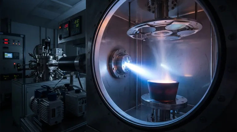
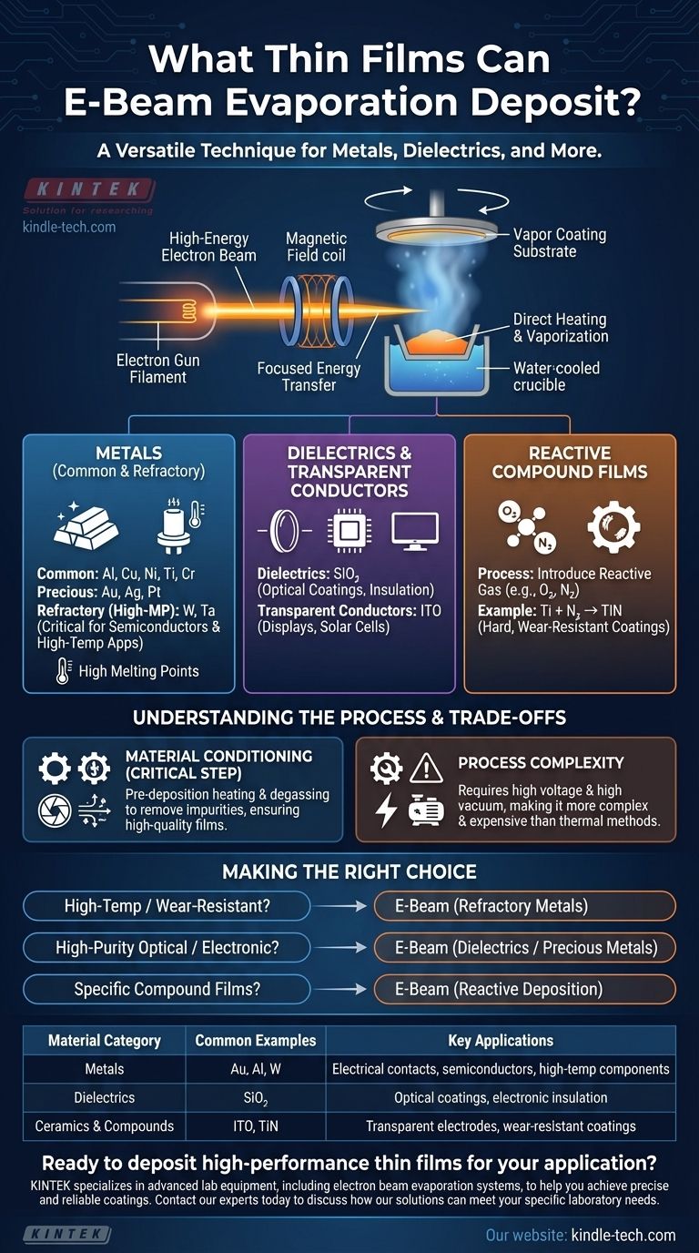
A current passes through a tungsten filament, which emits electrons. A high-voltage field accelerates these electrons, and a magnetic field focuses them into a tight beam aimed at the material to be deposited, which sits in a water-cooled crucible.
This concentrated energy transfer causes the target material to evaporate or sublimate directly, turning into a vapor that travels upwards and coats the substrate. This process is what enables the deposition of materials with extremely high melting points.
Metals: From Common to Refractory
E-beam is widely used for depositing a variety of metallic films.
This includes common metals like aluminum (Al), copper (Cu), nickel (Ni), titanium (Ti), and chromium (Cr). It is also a preferred method for precious metals such as gold (Au), silver (Ag), and platinum (Pt) due to its efficient material use.
However, its key strength is the ability to deposit refractory metals—materials with exceptionally high melting points. Examples include tungsten (W) and tantalum (Ta), which are critical in semiconductor and high-temperature applications.
Dielectrics and Transparent Conductors
The technique is not limited to metals. E-beam evaporation is frequently used to deposit dielectric materials, which are electrical insulators vital for optical coatings and electronic devices.
Common examples include silicon dioxide (SiO₂) and other ceramic-like compounds. It is also used for transparent conductive oxides like Indium Tin Oxide (ITO), which is essential for displays and solar cells.
Creating Compound Films with Reactive Gases
The versatility of e-beam can be extended even further through reactive deposition. By introducing a controlled amount of a reactive gas, such as **oxygen (O₂) or nitrogen (N₂) **, into the vacuum chamber during evaporation, it's possible to form compound films.
For example, evaporating titanium in a nitrogen environment can create a hard, wear-resistant titanium nitride (TiN) film on the substrate.
Understanding the Process Trade-offs
While powerful, achieving a high-quality film with e-beam evaporation requires careful process control. It is not a simple "plug-and-play" method.
The Importance of Material Conditioning
Before deposition begins, a shutter is placed over the source material. The e-beam is activated at a low power to heat, degas, and stabilize the evaporant.
This "conditioning" step is critical. It removes trapped gases and impurities from the source material that could otherwise be released during deposition, causing defects or "spitting" that ruins the film's quality.
Process Complexity
The need for high voltage, powerful magnetic fields for beam steering, and a high-vacuum environment makes the equipment more complex and expensive than simpler methods like thermal evaporation. This complexity is the necessary trade-off for its versatility and ability to handle difficult materials.
Making the Right Choice for Your Goal
The material you can deposit depends entirely on your application's requirements.
- If your primary focus is high-temperature electronics or wear-resistant coatings: E-beam is the superior choice for depositing refractory metals like tungsten and tantalum.
- If your primary focus is high-purity optical or electronic films: E-beam provides excellent control for depositing dielectrics like silicon dioxide and metals like gold or aluminum.
- If your primary focus is creating specific compound films: Use e-beam with a reactive gas to form specialized materials like oxides and nitrides directly on your substrate.
Ultimately, electron beam evaporation provides a precise and powerful path for turning a vast range of solid materials into high-performance thin films.
Summary Table:
| Material Category | Common Examples | Key Applications |
|---|---|---|
| Metals | Gold (Au), Aluminum (Al), Tungsten (W) | Electrical contacts, semiconductors, high-temp components |
| Dielectrics | Silicon Dioxide (SiO₂) | Optical coatings, electronic insulation |
| Ceramics & Compounds | Indium Tin Oxide (ITO), Titanium Nitride (TiN) | Transparent electrodes, wear-resistant coatings |
Ready to deposit high-performance thin films for your application?
KINTEK specializes in advanced lab equipment, including electron beam evaporation systems, to help you achieve precise and reliable coatings for metals, dielectrics, and ceramics. Our expertise supports critical applications in semiconductors, optics, and research.
Contact our experts today to discuss how our solutions can meet your specific laboratory needs.
Visual Guide
Related Products
- Electron Beam Evaporation Coating Oxygen-Free Copper Crucible and Evaporation Boat
- Molybdenum Tungsten Tantalum Evaporation Boat for High Temperature Applications
- Aluminized Ceramic Evaporation Boat for Thin Film Deposition
- Tungsten Evaporation Boat for Thin Film Deposition
- Electron Beam Evaporation Coating Tungsten Crucible and Molybdenum Crucible for High Temperature Applications
People Also Ask
- How is an electron beam evaporator cooled during deposition? Essential Thermal Management for Stable Processes
- What is e-beam evaporation used for? Precision Coating for Optics, Aerospace & Electronics
- What are the applications of e-beam evaporation? Achieve High-Purity Coatings for Optics & Electronics
- What is the temperature of e-beam evaporation? Mastering the Two-Zone Thermal Process for Precision Films
- What is the current of e-beam evaporation? A Guide to High-Purity Thin Film Deposition


