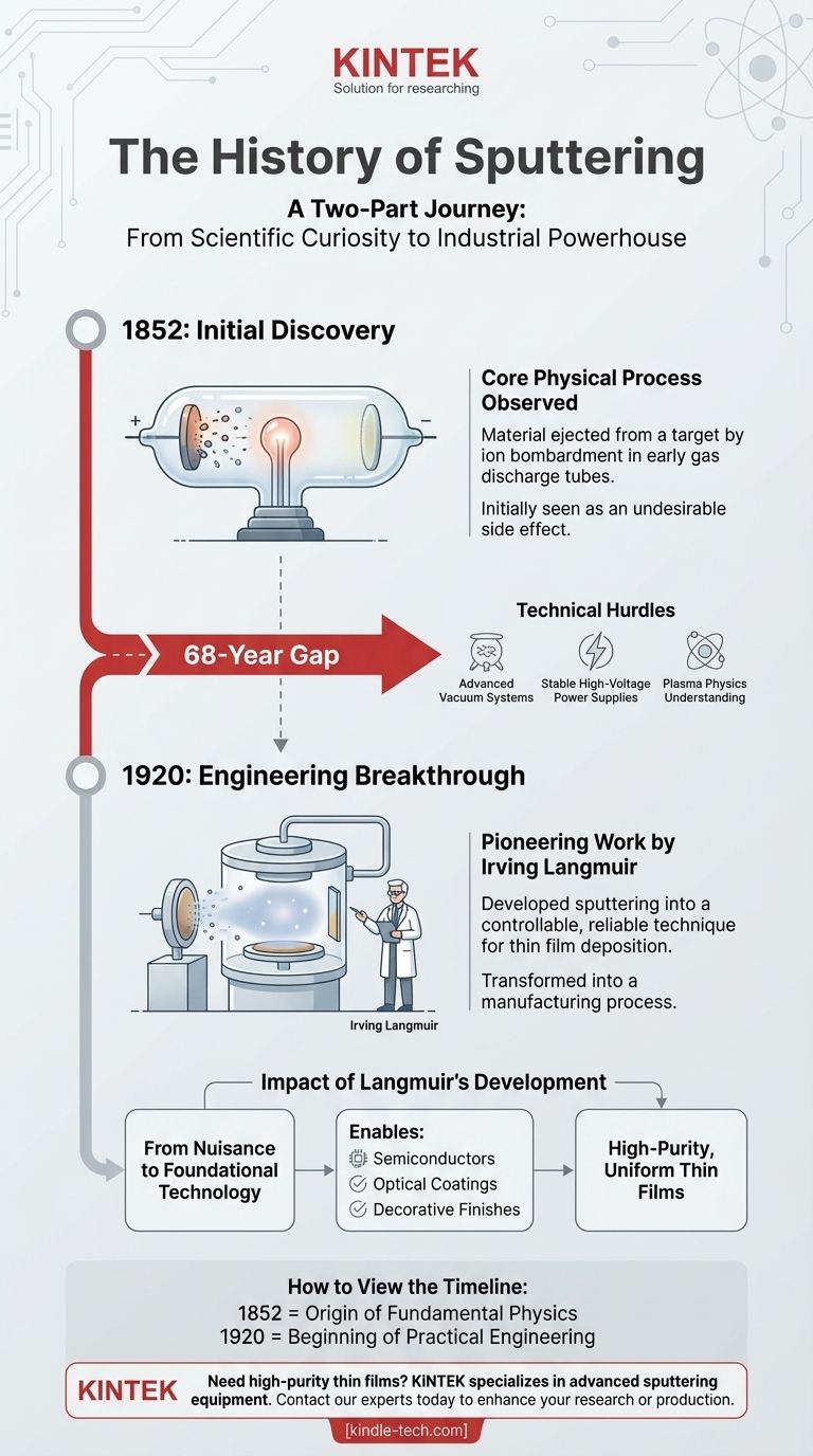
The invention of sputtering is best understood as a two-part history. The fundamental physical mechanism was first discovered in 1852, but it was not developed into a practical technique for depositing thin films until Irving Langmuir's work in 1920. This distinction separates the scientific observation from the engineering innovation.
Sputtering’s history highlights a crucial distinction in technology: the initial discovery of a physical phenomenon is often separated by decades from the engineering work required to turn it into a reliable, controllable process.
The Two-Part History of Sputtering
Understanding the timeline requires separating the moment the effect was first seen from the moment it was harnessed for a specific purpose.
The Initial Discovery (1852)
The core physical process of sputtering—whereby atoms are ejected from a solid target material due to bombardment by energetic ions—was first observed in 1852.
This discovery was a byproduct of early experiments with gas discharges in vacuum tubes. Scientists noticed that material from the cathode (the negative electrode) was being eroded and deposited elsewhere inside the tube, but it was initially viewed as an undesirable side effect.
The Engineering Breakthrough (1920)
It took 68 years for the phenomenon to be intentionally developed into a useful technology. In 1920, pioneering chemist and physicist Irving Langmuir developed sputtering as a controlled method for thin film deposition.
Langmuir's work marked the true invention of sputter deposition as a manufacturing process. He established the principles for using a plasma to create a controlled ion bombardment, allowing for the precise and uniform coating of a substrate with material from a target.
From Scientific Curiosity to Industrial Process
The long gap between the discovery of the sputtering effect and its application as a deposition tool underscores the significant technical hurdles that had to be overcome.
Why the 68-Year Gap?
The initial observation in 1852 was just that—an observation. Turning it into a repeatable, industrial process required advancements in several parallel technologies.
This included the development of much more advanced vacuum systems to control the purity of the environment, highly stable high-voltage power supplies to sustain a consistent plasma, and a deeper theoretical understanding of plasma physics.
The Impact of Langmuir's Development
Langmuir's work transformed sputtering from a nuisance into a foundational technology. By creating a controllable process, he unlocked the ability to deposit thin, high-purity films with excellent adhesion and uniformity.
This breakthrough laid the groundwork for countless modern applications, from creating the microscopic circuitry in semiconductors to applying anti-reflective coatings on optical lenses and durable decorative finishes on consumer products.
How to View Sputtering's Timeline
To properly contextualize the invention, consider the goal of your inquiry.
- If your primary focus is on fundamental physics: The 1852 discovery marks the origin point for understanding the core science of ion-solid interactions.
- If your primary focus is on manufacturing and technology: The 1920 development by Langmuir is the true beginning of sputter deposition as a practical engineering process.
Ultimately, appreciating both milestones is key to understanding the complete journey of this critical technology from a laboratory curiosity to an industrial powerhouse.
Summary Table:
| Year | Event | Key Figure/Context |
|---|---|---|
| 1852 | Initial Discovery | Observed as erosion in gas discharge tubes |
| 1920 | Engineering Breakthrough | Irving Langmuir developed controlled deposition |
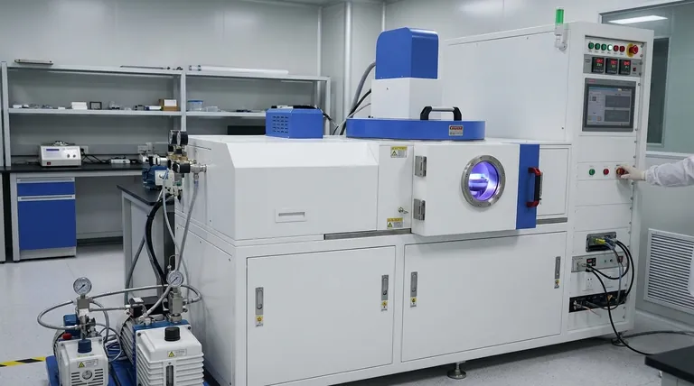
Need high-purity thin films for your lab? KINTEK specializes in advanced sputtering equipment and consumables, providing the reliable, controllable deposition processes that industries rely on. Contact our experts today to discuss how our solutions can enhance your research or production line.
Visual Guide
Related Products
- Spark Plasma Sintering Furnace SPS Furnace
- Vacuum Induction Melting Spinning System Arc Melting Furnace
- Chemical Vapor Deposition CVD Equipment System Chamber Slide PECVD Tube Furnace with Liquid Gasifier PECVD Machine
- Customer Made Versatile CVD Tube Furnace Chemical Vapor Deposition Chamber System Equipment
People Also Ask
- What is SPS sintering method? A Guide to High-Speed, High-Performance Material Fabrication
- What is the pressure for spark plasma sintering? A Guide to Optimizing SPS Parameters
- What is the difference between spark plasma sintering and flash sintering? A Guide to Advanced Sintering Methods
- What are the fundamentals of spark plasma sintering process? Unlock Rapid, High-Performance Material Consolidation
- What is the mechanism of SPS process? A Deep Dive into Rapid, Low-Temperature Sintering


