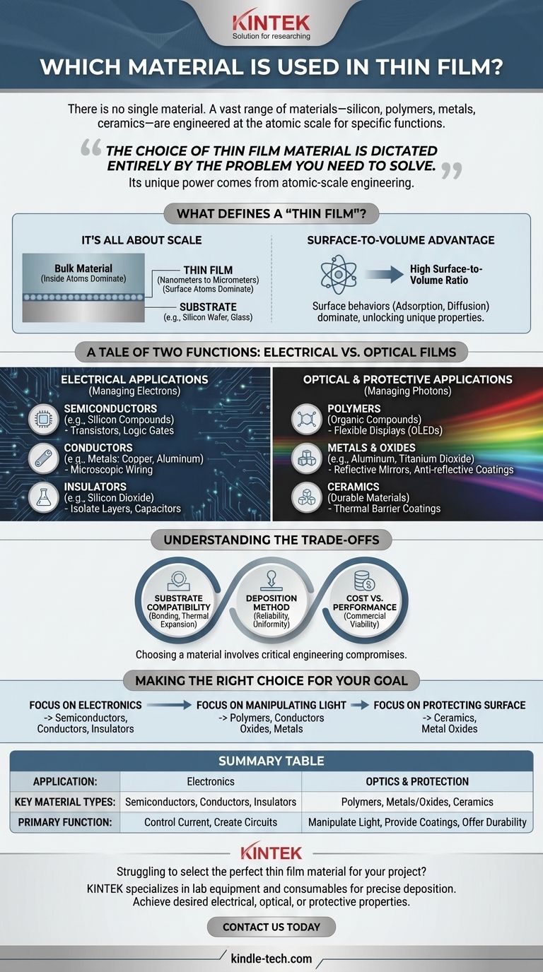
There is no single material used for thin films. Instead, a vast range of materials—including silicon, polymers, metals, and ceramics—are chosen based on the film's intended function, whether it's for electronics, optics, or protective coatings. The defining characteristic is not the material itself, but its deposition in an extremely thin layer, often just nanometers to micrometers thick.
The choice of a thin film material is dictated entirely by the problem you need to solve. The unique power of a thin film comes from engineering a material at an atomic scale, where its properties can be fundamentally different from its bulk form.
What Defines a "Thin Film"?
Before examining specific materials, it's critical to understand what makes a thin film unique. The material's behavior changes dramatically when its structure is reduced to a nearly two-dimensional form.
It's All About Scale
A thin film is a layer of material deposited onto a surface, known as a substrate (like glass or a silicon wafer).
Its thickness is measured in nanometers or micrometers, making it thousands of times thinner than its length or width.
The Surface-to-Volume Advantage
In bulk materials, the properties are determined by the vast number of atoms inside. In a thin film, the surface-to-volume ratio is extremely high.
This means that surface-level atomic behaviors, such as adsorption and diffusion, dominate the material's overall properties. This shift is what unlocks the unique electrical, optical, and mechanical characteristics used in advanced technology.
A Tale of Two Functions: Electrical vs. Optical Films
The easiest way to categorize thin film materials is by their primary application. Most uses fall into either managing electrons (electrical) or managing photons (optical and protective).
Materials for Electrical Applications
These films form the foundation of modern electronics, where materials are chosen for their ability to control the flow of electrical current.
- Semiconductors: Crystalline materials like silicon compounds are the backbone of the industry. They are used to create the transistors and logic gates found in integrated circuits and microprocessors.
- Conductors: Thin films of metals like copper or aluminum are deposited to create the microscopic wiring that connects components within an integrated circuit.
- Insulators: Dielectric materials like silicon dioxide are used to isolate conductive layers, preventing short circuits and enabling the construction of capacitors and other components.
Materials for Optical and Protective Applications
These films are designed to interact with light or protect a substrate from the environment.
- Polymers: Organic polymer compounds are increasingly used for their flexibility and tunable optical properties. They are essential for modern technologies like flexible solar cells and Organic Light Emitting Diodes (OLEDs) used in high-end displays.
- Metals and Oxides: Different metals and metal oxides are used for their ability to manipulate light. A thin layer of aluminum can create a highly reflective mirror, while layers of titanium dioxide can create an anti-reflective coating for lenses.
- Ceramics: Extremely durable materials are used to create thermal barrier coatings, such as those that protect turbine blades in the aerospace industry.
Understanding the Trade-offs
Choosing a thin film material is not just about its primary function. It involves a series of critical engineering compromises.
The Substrate Matters
A thin film is only as good as its bond to the substrate. The chosen material must adhere well and have a compatible thermal expansion coefficient to prevent cracking or peeling when temperatures change.
The Deposition Method Is Key
Materials can only be used if a reliable deposition method exists to create a uniform, thin layer. Some high-performance materials are difficult or expensive to deposit, limiting their practical application.
Cost vs. Performance
In any commercial application, performance must be balanced against cost. While an exotic material might offer superior properties, a more common material like silicon might provide the necessary performance at a fraction of the cost.
Making the Right Choice for Your Goal
The material you choose is a direct reflection of your objective.
- If your primary focus is creating electronic devices: You will be working with semiconductors like silicon, conductors like metals, and insulators like specific oxides.
- If your primary focus is manipulating light: Your key materials will be polymers for flexible displays, transparent conductive oxides for touch screens, and various metals for their reflective or anti-reflective properties.
- If your primary focus is protecting a surface: You will look toward highly durable ceramics and specific metal oxides to create thermal, chemical, or wear-resistant barriers.
Ultimately, the power of thin films lies not in a single material, but in the principle of engineering materials at the atomic scale to achieve extraordinary properties.
Summary Table:
| Application | Key Material Types | Primary Function |
|---|---|---|
| Electronics | Semiconductors (e.g., Silicon), Conductors (e.g., Copper), Insulators (e.g., Silicon Dioxide) | Control electrical current, create circuits, and prevent shorts |
| Optics & Protection | Polymers, Metals/Oxides (e.g., Aluminum, Titanium Dioxide), Ceramics | Manipulate light, provide reflective/anti-reflective coatings, and offer durability |
Struggling to select the perfect thin film material for your project? KINTEK specializes in lab equipment and consumables for precise thin film deposition. Our expertise ensures you achieve the desired electrical, optical, or protective properties for your application. Contact us today to discuss your specific needs and optimize your thin film process!
Visual Guide