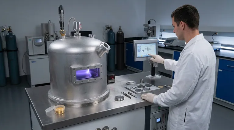
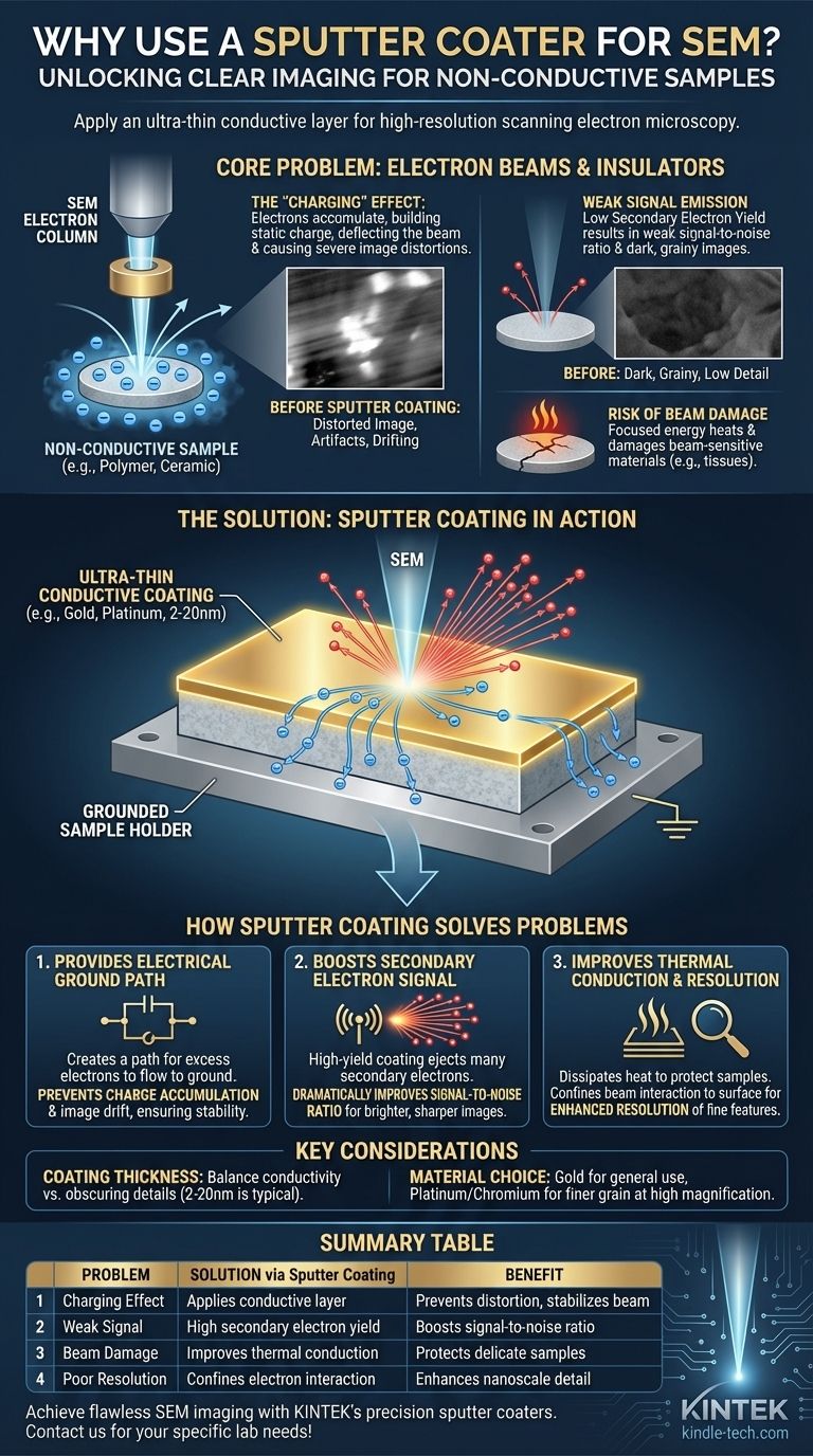
In Scanning Electron Microscopy (SEM), a sputter coater is used to apply an ultra-thin, electrically conductive layer onto non-conductive samples. This essential preparation step is what makes it possible to acquire clear, high-resolution images of materials like ceramics, polymers, and biological specimens, which would otherwise produce distorted and unusable results.
The core function of sputter coating is to solve a fundamental problem: the electron beam used by an SEM will accumulate on the surface of a non-conductive sample, causing a "charging" effect that catastrophically distorts the image. The conductive coating provides a path for this charge to dissipate to ground, enabling stable and accurate imaging.
The Core Problem: Electron Beams and Insulators
To understand the need for sputter coating, you must first understand how an SEM interacts with a sample that cannot conduct electricity. This interaction creates several critical imaging issues.
The "Charging" Effect
When the SEM's primary electron beam strikes a non-conductive surface, those electrons have nowhere to go. They accumulate on the sample, building up a negative static charge.
This localized charge deflects the incoming electron beam, causing severe image artifacts. You will often see bright patches, distorted features, or a drifting image, making meaningful analysis impossible.
Weak Signal Emission
The image in an SEM is primarily generated by detecting secondary electrons that are ejected from the sample's surface by the primary beam.
Many non-conductive materials are inherently poor emitters of these secondary electrons. This results in a weak signal and a low signal-to-noise ratio, producing a dark, grainy, and indistinct image.
Risk of Beam Damage
The focused energy of the electron beam can heat and damage delicate or "beam-sensitive" samples. This is a significant concern for polymers, organic tissues, and other soft materials, which can be altered or destroyed by the microscope itself.
How Sputter Coating Solves These Problems
Applying a thin metal film, typically just 2-20 nanometers thick, directly counteracts each of these issues and dramatically improves image quality.
Providing an Electrical Ground Path
The most important benefit is that the conductive coating—often gold, platinum, or iridium—creates a path for the excess electrons to flow away from the imaged area and down to the grounded SEM sample holder.
This prevents charge accumulation entirely, stabilizing the image and eliminating the distortions common to non-conductive samples.
Boosting the Secondary Electron Signal
The metals used for sputter coating are chosen because they have a very high secondary electron yield. When the primary beam hits this coating, it ejects a large number of secondary electrons.
This flood of new signal dramatically improves the signal-to-noise ratio. The result is a much brighter, sharper, and more detailed image that reveals the true surface topography of the underlying specimen.
Improving Thermal Conduction and Resolution
The metal coating also helps to dissipate heat away from the analysis area, offering a layer of protection for beam-sensitive specimens.
Furthermore, the coating reduces the penetration depth of the primary electron beam. This confines the interaction to the very near-surface region, which can improve the resolution of fine surface features and edges.
Understanding the Trade-offs
While essential, the sputter coating process is not without its own considerations. Achieving the best results requires balancing competing factors.
Coating Thickness is Critical
The thickness of the sputtered layer is a crucial parameter. A layer that is too thin will not be fully conductive and will fail to prevent charging.
Conversely, a layer that is too thick will begin to obscure the fine nanoscale details of your sample's actual surface. The goal is to apply the thinnest possible continuous film that effectively dissipates charge.
The Choice of Material Matters
Different coating materials are used for different applications. Gold is a common and effective choice for general imaging due to its high conductivity and secondary electron yield.
However, other materials like gold/palladium, platinum, or chromium produce a finer grain structure in the coating, which is often necessary for achieving the highest magnifications without seeing the texture of the coating itself.
How to Apply This to Your Sample
Your decision to use a sputter coater should be based on the nature of your sample and your imaging goals.
- If your sample is a non-conductor (ceramic, polymer, glass, most biological tissue): Sputter coating is almost always required to prevent charging and acquire a usable image.
- If your sample is beam-sensitive: The conductive coating provides critical thermal and electrical protection that can prevent damage during analysis.
- If you need the highest possible image resolution: Even on poorly-conducting materials, a thin coating will significantly improve the signal-to-noise ratio, revealing fine surface details that would otherwise be lost in the noise.
Ultimately, sputter coating is a foundational technique that transforms an SEM from a tool for conductive materials into a universally powerful instrument for exploring the micro and nano-scale world of nearly any sample.
Summary Table:
| Problem | Solution via Sputter Coating | Benefit |
|---|---|---|
| Charging Effect | Applies conductive layer (e.g., Au, Pt) | Prevents image distortion, stabilizes beam |
| Weak Signal Emission | High secondary electron yield of metal coating | Boosts signal-to-noise ratio for sharper images |
| Beam Damage Risk | Improves thermal conduction | Protects delicate, beam-sensitive samples |
| Poor Resolution | Confines electron interaction to surface | Enhances detail visibility of nanoscale features |
Achieve flawless SEM imaging with KINTEK's precision sputter coaters. Whether you're working with ceramics, polymers, or biological samples, our lab equipment ensures optimal coating thickness and material selection to eliminate charging and maximize image clarity. Let our experts help you enhance your microscopy results—contact us today to discuss your specific laboratory needs!
Visual Guide
Related Products
- Custom CVD Diamond Coating for Lab Applications
- HFCVD Machine System Equipment for Drawing Die Nano-Diamond Coating
- Chemical Vapor Deposition CVD Equipment System Chamber Slide PECVD Tube Furnace with Liquid Gasifier PECVD Machine
- Multifunctional Electrolytic Electrochemical Cell Water Bath Single Layer Double Layer
- Professional Cutting Tools for Carbon Paper Cloth Diaphragm Copper Aluminum Foil and More
People Also Ask
- What is CVD coating used for? Hardening Tools & Building Semiconductors for Industry
- How thick is CVD diamond coating? Balancing Durability and Stress for Optimal Performance
- What are the advantages of CVD coating? Superior Hardness and Uniformity for Demanding Applications
- What is CVD coating? Transform Your Material's Surface for Maximum Performance
- Can you coat something in diamond? Unlock Unmatched Hardness and Thermal Conductivity


