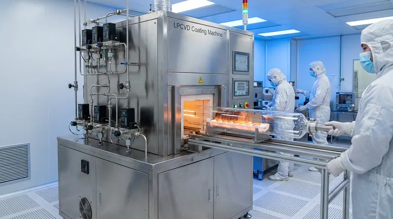
At its core, LPCVD is used to deposit exceptionally uniform and pure thin films over complex, three-dimensional surfaces. This capability makes it a cornerstone technology in the manufacturing of high-performance semiconductor devices, Micro-Electro-Mechanical Systems (MEMS), and modern solar cells, where the quality and consistency of these thin layers are paramount.
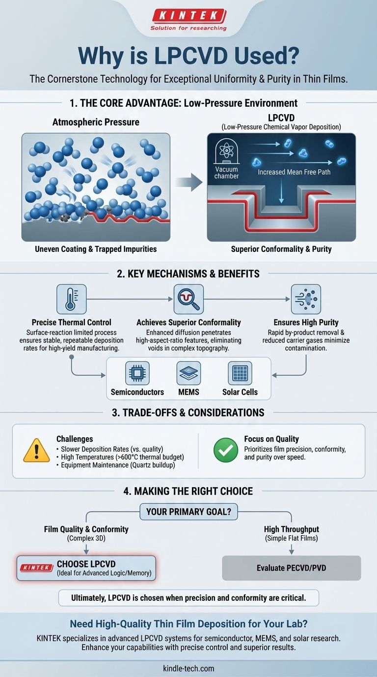
The fundamental advantage of LPCVD lies in its low-pressure environment. This condition allows reactive gases to spread out and coat all surfaces of a microscopic structure evenly before a chemical reaction takes place, ensuring superior film conformity and purity that atmospheric pressure methods cannot easily achieve.
The Fundamental Advantage: Control Through Low Pressure
The "low pressure" in LPCVD is not just a condition; it is the central principle that enables its most valuable characteristics. By reducing the pressure in the reaction chamber, we fundamentally change the behavior of the precursor gases.
How Low Pressure Drives Uniformity
In a low-pressure environment, gas molecules are farther apart and collide less frequently. This increases their mean free path—the average distance a molecule travels before hitting another.
As a result, the precursor gases diffuse rapidly throughout the chamber, reaching every wafer and every location on each wafer at nearly the same concentration. Because the deposition rate is primarily controlled by the surface temperature (which is very uniform), the resulting film thickness is exceptionally consistent across the wafer and from one wafer to the next.
Achieving Superior Conformality
Conformality is the ability of a film to maintain a uniform thickness as it coats an uneven surface, such as deep trenches or steps in a microchip.
LPCVD excels at this because the enhanced diffusion allows precursor gases to penetrate these high-aspect-ratio features completely. The gas molecules coat the bottom and sidewalls of a trench just as effectively as the top surface, which is critical for preventing voids and ensuring electrical isolation in modern integrated circuits.
The Role of Thermal Control
Most LPCVD processes are designed to be surface-reaction limited, not mass-transport limited. This means the bottleneck is the speed of the chemical reaction on the wafer surface, which is highly dependent on temperature.
Since temperature can be controlled with extreme precision, the deposition rate becomes very stable and predictable. This leads to excellent run-to-run repeatability, a non-negotiable requirement for high-yield manufacturing.
Ensuring High Purity
The low-pressure environment allows reaction by-products to be pumped out of the chamber quickly, preventing them from being incorporated back into the growing film as impurities.
Furthermore, LPCVD often eliminates the need for inert carrier gases (like nitrogen or argon) that are common in atmospheric pressure systems. This reduces a potential source of particle contamination, leading to a purer final film.
Understanding the Trade-offs and Limitations
No process is without its compromises. The high quality of LPCVD films comes with specific operational considerations.
Slower Deposition Rates
Because the process is often limited by surface reaction kinetics and uses lower concentrations of precursor gases, LPCVD can be slower than other deposition methods. This is a direct trade-off: sacrificing speed for superior film quality and conformity.
The Challenge of High Temperatures
LPCVD is a thermal process that often operates at high temperatures (600°C or higher). This thermal budget can be a limitation for device structures that contain materials with low melting points or that are sensitive to heat-induced changes.
Equipment and Maintenance Demands
The high-temperature process can cause the precursor gases to deposit on the internal quartz components of the reactor, not just the wafers. Over time, this buildup can flake off, creating particles, or cause stress that leads to component failure. Regular cleaning and maintenance are critical.
Operational Contamination Risks
While the process itself produces high-purity films, like any sensitive manufacturing process, it is susceptible to environmental contamination if not handled correctly. Proper cleanroom protocols are essential to prevent external contaminants, such as bacteria, from compromising the equipment or the devices.
Making the Right Choice for Your Goal
Selecting LPCVD is a strategic decision based on the specific technical requirements of the film you need to create.
- If your primary focus is film quality and conformity: LPCVD is the ideal choice for coating complex topographies with exceptional uniformity, as required for advanced logic and memory devices.
- If your primary focus is high throughput for simple, flat films: You may evaluate faster, less conformal methods like Plasma-Enhanced CVD (PECVD) or Physical Vapor Deposition (PVD), accepting the potential quality trade-offs.
- If your primary focus is cost-effective, large-scale production: LPCVD offers a mature, versatile, and high-quality process that is well-suited for applications like solar cells, where both performance and scalability are essential.
Ultimately, LPCVD is chosen when the precision, purity, and conformity of the resulting thin film are more critical than the sheer speed of deposition.
Summary Table:
| Feature | Advantage | Key Application |
|---|---|---|
| Low-Pressure Environment | Enhanced gas diffusion for uniform coating | Complex 3D structures in semiconductors |
| Thermal Control | Precise, repeatable deposition rates | High-yield manufacturing processes |
| High Conformality | Uniform film thickness on trenches and steps | Advanced microchips and MEMS devices |
| High Purity | Minimal contamination from by-products | Solar cells and high-performance electronics |
Need high-quality thin film deposition for your lab? KINTEK specializes in advanced lab equipment and consumables, including LPCVD systems designed for semiconductor, MEMS, and solar cell research. Our solutions ensure precise thermal control, superior film conformity, and minimal contamination—helping you achieve reliable, repeatable results. Contact us today to discuss how our expertise can enhance your laboratory's capabilities!
Visual Guide
Related Products
- Inclined Rotary Plasma Enhanced Chemical Vapor Deposition PECVD Equipment Tube Furnace Machine
- Inclined Rotary Plasma Enhanced Chemical Vapor Deposition PECVD Equipment Tube Furnace Machine
- Chemical Vapor Deposition CVD Equipment System Chamber Slide PECVD Tube Furnace with Liquid Gasifier PECVD Machine
- Laboratory CVD Boron Doped Diamond Materials
- Microwave Plasma Chemical Vapor Deposition MPCVD Machine System Reactor for Lab and Diamond Growth
People Also Ask
- How does the PECVD function enhance thin-film properties? Achieve Superior Chemical Stability & Durability
- What is plasma activated chemical vapour deposition method? A Low-Temperature Solution for Advanced Coatings
- What are the core advantages of PE-CVD in OLED encapsulation? Protect Sensitive Layers with Low-Temp Film Deposition
- What is the necessity of depositing a silicon nitride (SiNx) thin film using PECVD? Optimize QSSPC Lifetime Measurement
- What is plasma enhanced chemical vapour deposition PECVD used for? Enable Low-Temp Thin Films for Electronics & Solar


