Introduction to Thin Film Deposition
Thin film deposition is the process of depositing a thin layer of material onto a substrate. It is widely used in the manufacturing of electronic and optical devices such as integrated circuits, solar cells, and flat panel displays. The two most common techniques used for thin film deposition are evaporation and sputtering. In evaporation, the material is heated until it evaporates and condenses onto the substrate. In sputtering, the material is ejected from a target by bombarding it with high-energy ions. Both techniques have their advantages and disadvantages, and the choice of technique depends on the specific application.
Table of Contents
- Introduction to Thin Film Deposition
- Overview of Evaporation and Sputtering Techniques
- Evaporation Methods: Resistive Thermal and Electron-beam
- Sputtering Process: Gas Ionization and Target Bombardment
- Comparison of Evaporation and Sputtering
- Advantages and Disadvantages of Each Technique
- Applications and Uses of Evaporation and Sputtering
- Conclusion: which technique is best for thin film deposition
Overview of Evaporation and Sputtering Techniques
Thin film deposition is a vacuum technique used to apply coatings of pure materials onto the surface of various objects such as semiconductor wafers, optical components, solar cells, and many other possibilities. There are various forms of thin film deposition available, including physical vapor deposition (PVD) and sputtering.
Evaporation Technique
Evaporation is a PVD technique that involves heating a solid material in a vacuum chamber until it vaporizes and condenses onto a substrate. The technique falls under the PVD umbrella, and it consists of thermal evaporation, electron-beam evaporation, and inductive heating. Thermal evaporation is used to deposit metals for thin film transistors, solar cells, and OLEDs. Electron-beam evaporation is used in producing optical thin films such as glasses and solar panels. Inductive heating is seldom used in the nano/micro fabrication industry due to its lack of efficiency.
Evaporation is a simpler and more cost-effective technique, and it can produce films with high purity and uniformity. It is often used in the production of OLEDs, solar cells, and integrated circuits. However, it suffers from poor uniformity, the highest impurity levels of any PVD method, and moderate film stress.
Sputtering Technique
Sputtering is a PVD technique that involves bombarding a material with ions or high-energy particles to eject atoms or molecules that then condense onto a substrate. The technique is widely used to deposit metals and dielectrics. There are two types of sputtering: magnetron sputtering and ion beam sputtering.
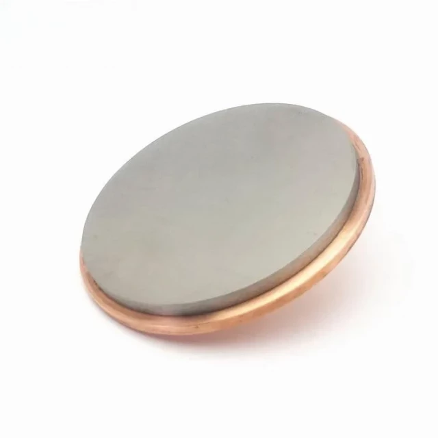
Magnetron sputtering involves introducing a controlled gas, typically chemically inert argon, into a vacuum chamber and then electrically energizing a cathode to generate a self-sustaining plasma. The exposed surface of the cathode, referred to as the target, is a piece of the material to be applied over the substrates. The gas atoms become positively charged ions by losing electrons within the plasma and are then accelerated with adequate kinetic energy to hit the target and dislocate atoms or molecules from the target material. This sputtered material now consists of a vapor stream, which passes through the chamber and strikes and sticks onto the substrate as a film or coating.
Ion beam sputtering is similar to magnetron sputtering but uses a beam of ions instead of a plasma. It produces films with higher density and better adhesion to the substrate. It can also be used to deposit a wider range of materials, including metals, ceramics, and polymers.
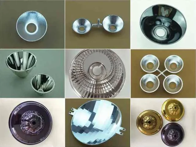
Sputtering is commonly used in the manufacture of hard disk drives, optical coatings, and thin-film solar cells. It can produce films with remarkable precision and high-quality films with less scatter than conventional evaporation. However, sputtering requires a more complex setup and is more expensive than evaporation.
Overall, both evaporation and sputtering have their own unique strengths and weaknesses. The choice of technique depends on the specific application and the desired properties of the thin film.
Evaporation Methods: Resistive Thermal and Electron-beam
Thin film deposition is an important process used in the manufacturing of various high-tech devices, including electronic devices, solar panels, and optical components. Two popular techniques for thin film deposition are evaporation and sputtering. In this section, we will discuss two types of evaporation methods commonly used in thin film deposition: resistive thermal evaporation and electron-beam evaporation.
Resistive Thermal Evaporation
Resistive thermal evaporation is a process that uses a resistive heating element to vaporize the material. This method involves placing the source material in a crucible made of passive material, such as boron nitride (BN), and an external heater. The heater is then used to heat the resistive material to its melting point, causing it to vaporize and condense onto a substrate to form a thin film. This process is typically carried out in a vacuum environment with a pressure of less than 10^-5 torr.
Resistive thermal evaporation is a relatively simple and low-cost method of thin film deposition. It is also a gentle technique that produces evaporated particle energies of approximately 0.12 eV or 1500 K. However, this method has some limitations, such as poor control over the deposition process.
Electron-beam Evaporation
Electron-beam evaporation is another technique used in thin film deposition. This method uses a high-energy electron beam to heat the material inside a water-cooled copper hearth or crucible. This process produces a very high temperature, which allows metals and dielectrics with high melting temperatures, such as gold and silicon dioxide, to be vaporized and deposited on a substrate to form a thin film.
Compared to resistive thermal evaporation, electron-beam evaporation has a better deposition rate and can produce high-quality thin films with a high degree of control. However, this method is more complex and requires a cooling system, which can decrease production rates and increase energy costs.
Comparison of Resistive Thermal and Electron-beam Evaporation
Both resistive thermal and electron-beam evaporation methods have their respective advantages and disadvantages. Resistive thermal evaporation is a simple and low-cost method of thin film deposition, but it has poor control over the deposition process. Electron-beam evaporation, on the other hand, offers better control over the deposition process and can produce high-quality thin films, but it is a more complex method that requires a cooling system.
Ultimately, the choice between these two techniques depends on the specific requirements of the thin film application and the available resources. A comparative study of evaporation and sputtering techniques can help researchers and manufacturers to better understand the advantages and limitations of each method and make informed decisions in the thin film deposition process.
Sputtering Process: Gas Ionization and Target Bombardment
Sputtering is a physical process that involves the ejection of atoms from a solid target material into the gas phase. It is commonly used in the manufacturing of electronic devices to deposit a thin film onto a substrate. This process is carried out in a vacuum chamber where the target material is bombarded with energetic ions, causing atoms to be ejected from the target surface.
Gas Ionization
The sputtering process involves the use of gas ionization to create a plasma. The gas used in the process is typically argon, which is ionized by applying a high voltage to it. This creates a plasma of positively charged ions and electrons, which are then accelerated towards the target material.
Target Bombardment
Once the plasma is created, the positively charged ions are accelerated towards the target material. When the ions collide with the target surface, they transfer their energy to the atoms in the target material, causing them to be ejected from the surface. These ejected atoms then travel through the vacuum chamber and deposit onto the substrate, forming a thin film.
Sputter Yield
The efficiency of the sputtering process is measured by the sputter yield, which is the number of atoms ejected from the surface per incident ion. The sputter yield depends on several factors, including the energy of the incident ions, the mass of the ions and target atoms, and the binding energy of atoms in the solid.
Control Over Thin Film Thickness and Composition
One of the advantages of the sputtering process is the ability to have greater control over the thickness and composition of the thin film. The process allows for the deposition of multiple layers, enabling the creation of complex thin film structures. This level of control is not possible with other deposition techniques, such as evaporation.
Wide Range of Materials
Sputtering is also capable of depositing a wider range of materials compared to evaporation. This includes metals, ceramics, and semiconductors. This makes sputtering a more versatile technique for thin film deposition in the electronics industry.
In summary, the sputtering process involves the use of gas ionization and target bombardment to deposit a thin film onto a substrate. This process allows for greater control over the thickness and composition of the film, as well as the ability to deposit a wider range of materials. These advantages make sputtering a more efficient and precise method compared to evaporation for thin film deposition in the electronics industry.
Comparison of Evaporation and Sputtering
Thin film deposition techniques are vital for various scientific and industrial applications. Two commonly used techniques for thin film deposition are evaporation and sputtering. In this section, we will compare these two techniques based on various factors such as material properties, film thickness, and application requirements.
Material Properties
Evaporation is limited by the types of materials that can be evaporated. On the other hand, sputtering allows for a wider range of materials to be deposited, making it a more versatile technique.
Film Thickness
Evaporation is a relatively simple and cost-effective method that involves heating a source material until it vaporizes and condenses onto a substrate to form a thin film. However, it is limited by the thickness and uniformity of the resulting films. Sputtering, on the other hand, allows for better control over film thickness and composition. The thickness can be controlled by easily adjusting the deposition time.
Film Quality
Sputtering generally produces films with higher density and smoother surfaces compared to evaporation. This is because sputtering allows for more energetic and directional deposition of atoms, resulting in fewer defects and impurities in the films. However, evaporation can be advantageous in certain applications where a more porous or rough surface is desired.
Cost and Complexity
Evaporation is a relatively simple and cost-effective method compared to sputtering. However, sputtering can deposit a wider range of materials with better control over film thickness and composition, but it can be more complex and expensive to set up and maintain than evaporation.
Applications
The choice between evaporation and sputtering depends on various factors such as the material properties, film thickness, and application requirements. For example, if a more porous or rough surface is desired, then evaporation can be advantageous. On the other hand, if high-quality films with better control over thickness and composition are required, then sputtering is the better choice.
In conclusion, both evaporation and sputtering have their own advantages and disadvantages. A comparative study of the two techniques can help researchers choose the most suitable method for their specific applications.
Advantages and Disadvantages of Each Technique
Evaporation
- Simple and cost-effective technique.
- Can be used to deposit a wide range of materials.
- Offers high deposition rates.
- Good adhesion to the substrate.
- Can be used to deposit thick films.
- Limited by low deposition rates.
- Poor adhesion to the substrate.
- More difficult to control the film composition.
- Absence of capability to do in situ cleaning of substrate surfaces.
- Step coverage is more difficult to improve.
Sputtering
- Offers higher deposition rates.
- Better adhesion to the substrate.
- Greater control over film thickness and composition.
- Operates under lesser vacuum range.
- Can be used to deposit a wide range of materials.
- More complex and expensive process.
- Requires the use of specialized equipment.
- High capital expenses are required.
- The rates of deposition of some materials are relatively low.
- Sputtering has a greater tendency to introduce impurities in the substrate.
- Some materials such as organic solids are easily degraded by ionic bombardment.
- X-ray damage caused by electron beam evaporation can occur.
Choosing the Appropriate Technique
The choice of technique will depend on the specific requirements of the application, such as the desired film thickness, composition, and properties. Both techniques have their advantages and disadvantages, and understanding the differences between these techniques is critical in selecting the most appropriate method for each application. For instance, evaporation can be used for depositing thick films and better step coverage, while sputtering can be used for better adhesion to the substrate and greater control over film thickness and composition. Moreover, sputtering is preferred when contamination is a concern and higher deposition rates are required.
Applications and Uses of Evaporation and Sputtering
Thin film deposition using evaporation and sputtering techniques is widely used in various industrial applications. Both methods have unique advantages and disadvantages that make them suitable for specific applications.
Applications of Evaporation
Evaporation is commonly used in the production of organic electronic devices such as OLEDs and solar cells. It is also used in the electronics industry to create thin film coatings for conducting, insulating, and protective layers on semiconductor devices. The optics industry also uses evaporative deposition to create thin film coatings for lenses and other optical components to improve their performance. Additionally, evaporative deposition is used in the aerospace industry to create thin film coatings for jet engine parts to improve their wear resistance and durability.
Applications of Sputtering
Sputtering is frequently used in the production of hard coatings for cutting tools and wear-resistant coatings for machine parts. It is also preferred for depositing high-melting-point materials, making it suitable for applications that require greater morphological quality of surfaces where roughness, grain size, stoichiometry, and other requirements are more significant than the deposition rate. Sputtering is also used in the production of thin film coatings for magnetic storage devices, optical coatings, and semiconductor devices.
Advantages of Evaporation and Sputtering
Both evaporation and sputtering techniques have their unique advantages that make them suitable for various applications. Evaporation, for example, allows for precise control of the thickness and composition of the deposited film. It is also suitable for depositing materials that have a low melting point. On the other hand, sputtering allows for the deposition of high-melting-point materials and is preferred for applications that require greater morphological quality of surfaces. It is also a more versatile method of thin film deposition as it can be used to deposit a wide range of materials and can be adapted to many different applications.
In conclusion, both evaporation and sputtering techniques are widely used in various industrial applications. Understanding the differences between these techniques is crucial in the development of new and advanced electronic devices. The choice between evaporation and sputtering depends on the specific application and the material to be deposited. Proper control of the deposition process is essential for producing high-quality thin films with the desired properties and performance.
Conclusion: which technique is best for thin film deposition
In conclusion, both evaporation and sputtering techniques have their advantages and disadvantages in thin film deposition. Evaporation is a simpler and more cost-effective method, but it is limited in its ability to deposit certain materials and may result in lower film quality. On the other hand, sputtering is a more versatile and precise technique, but it is more complex and expensive. The choice between the two methods ultimately depends on the specific requirements of the application. In general, if a higher quality film is required, sputtering would be the preferred method, but if cost and simplicity are the main considerations, then evaporation would be the better option.