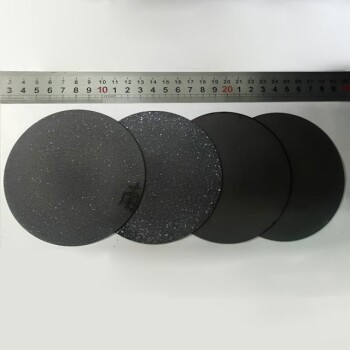
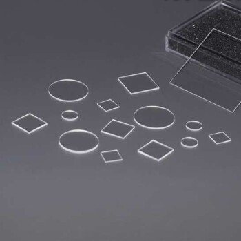
Introduction to PECVD Coating in Solar Cells
Market Demand and Importance of PECVD
As the market evolves, the demand for both performance and aesthetic appeal in crystalline silicon solar cells has surged. This shift has elevated the importance of PECVD (Plasma-Enhanced Chemical Vapor Deposition) coating, making it a pivotal factor in determining the quality and efficiency of these solar cells.
PECVD systems are indispensable tools in contemporary semiconductor manufacturing, renowned for their ability to produce films with exceptional uniformity, processed at low temperatures, and with high throughput. These characteristics make PECVD a cornerstone technology in various applications, including the deposition of thin films for microelectronic devices, photovoltaic cells, and display panels.
The PECVD process is particularly advantageous due to the superior physical properties of the films it produces. These films are not only uniform and highly cross-linked but also exhibit remarkable resistance to chemical and thermal changes. The cost-effectiveness and high efficiency of plasma-applied polymers have broadened the scope of PECVD applications, particularly in optical coatings and dielectric films.
Moreover, PECVD offers precise control over material properties such as stress, refractive index, and hardness, which are critical for the semiconductor industry. Films produced via PECVD are utilized for device encapsulation, surface passivation, and conductive layer isolation, further underscoring its significance in advancing the semiconductor sector.
In summary, as the demand for advanced electronic devices continues to escalate, the role of PECVD systems in the semiconductor industry is poised to become increasingly vital. This technology not only meets the evolving market needs for high-performance solar cells but also drives innovation in various other electronic applications.
Manufacturing Process and Role of PECVD
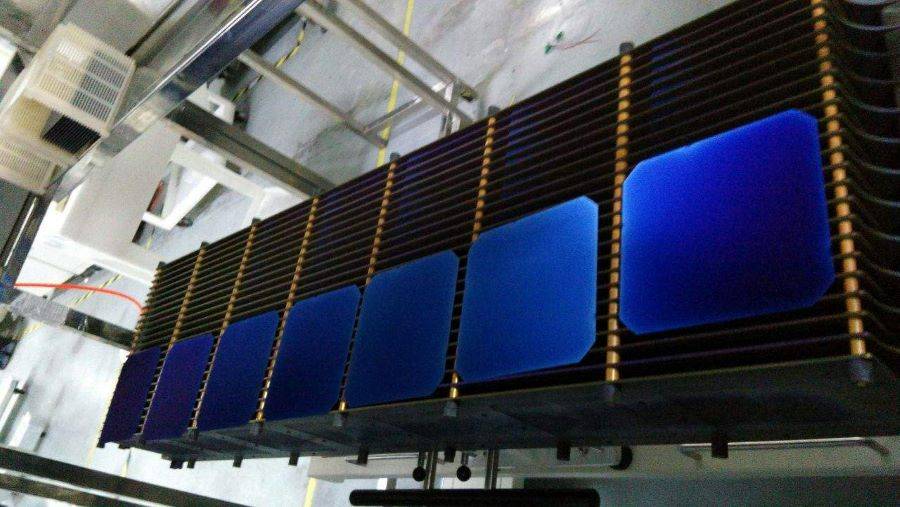
The manufacturing process of crystalline silicon solar cells is a multi-step procedure, with Plasma-Enhanced Chemical Vapor Deposition (PECVD) playing a pivotal role in both the aesthetic and economic aspects of solar cell production. PECVD is integral to the formation of high-quality, uniform films that enhance the solar cell's durability and efficiency, thereby reducing overall production costs.
PECVD-deposited films are renowned for their exceptional physical properties, such as uniformity, high cross-linking, and resistance to chemical and thermal changes. This technology is not only cost-effective but also highly efficient, making it a preferred method for creating optical coatings and dielectric films. The process allows for precise control over material properties, including stress, refractive index, and hardness, which are crucial for applications in the semiconductor industry. Films produced by PECVD are essential for device encapsulation, surface passivation, and conductive layer isolation, all of which are critical for the functionality and longevity of solar cells.
At a microscopic level, the PECVD process involves several intricate steps:
- Gas Activation: Gas molecules collide with electrons in the plasma to produce active groups and ions, though the formation of ions is less likely due to the higher energy required for ionization.
- Direct Diffusion: Active groups can diffuse directly to the substrate, initiating the deposition process.
- Chemical Interaction: Reactive groups interact with other gas molecules or reactive groups to form the necessary chemical groups for deposition.
- Surface Diffusion: The required chemical groups diffuse to the substrate surface.
- Direct Gas Diffusion: Some gas molecules may diffuse directly to the substrate vicinity without undergoing the activation process.
- System Discharge: Unreacted gas molecules are discharged out of the system.
- Deposition Reactions: Various chemical groups reaching the substrate surface undergo deposition reactions, releasing reaction products.
The applications of PECVD technology are vast and continually expanding. It is used to manufacture a variety of films, including insulating and passivating films like plasma silicon nitride films, amorphous silicon solar cells, polymer films, wear-resistant and corrosion-resistant TiC films, and aluminum oxide barrier films. Compared to other chemical vapor deposition methods, PECVD offers superior film uniformity and surface quality, making it an indispensable tool in the production of high-performance solar cells.
Common Rework Issues in PECVD Coating
Overview of Reworked PECVD Wafers
PECVD coating is a critical process in the production of crystalline silicon solar cells, primarily involving the generation of a Si3N4 film. This film is essential for enhancing the performance and durability of the solar cells. However, the rework process associated with PECVD coating often presents several common issues that can hinder the quality and efficiency of the final product.
One of the most noticeable issues is color differences across the wafer surface. These differences can occur due to variations in the deposition process, leading to inconsistent film thickness and composition. Another frequent problem is the presence of spots, which can be caused by impurities or defects in the coating material. Watermarks are also a common issue, often resulting from improper handling or storage conditions after the coating process.
In addition to these cosmetic issues, scratches and silicon removal are significant concerns. Scratches can occur during the handling or processing of the wafers, while silicon removal might happen due to over-etching or improper cleaning procedures. Each of these issues not only affects the visual appearance of the solar cells but also their overall performance and lifespan.
Addressing these rework issues is crucial for maintaining high-quality standards and reducing manufacturing costs. By understanding the root causes and implementing effective solutions, manufacturers can significantly improve the consistency and reliability of their PECVD coating processes.

Specific Rework Causes and Solutions
PECVD coating issues in crystalline silicon solar cells are multifaceted, requiring detailed analysis and targeted solutions. Key problems include edge color difference, center color difference, scratches, silicon removal, and abnormal discharge. Each of these issues can significantly impact the quality and performance of the solar cells.
-
Edge Color Difference: This often arises due to uneven deposition of the Si3N4 film. Solutions involve optimizing the gas flow rate and adjusting the temperature distribution across the wafer surface.
-
Center Color Difference: Similar to edge color difference, this issue can be mitigated by refining the PECVD process parameters, such as the pressure and the power applied during the deposition.
-
Scratches: These are typically caused by mechanical handling errors. Implementing stricter quality control measures and using more robust handling equipment can prevent this issue.
-
Silicon Removal: Improper etching can lead to unnecessary silicon removal. Adjusting the etching time and the concentration of the etching solution can address this problem.
-
Abnormal Discharge: This can be a result of irregular plasma formation. Ensuring stable plasma conditions by maintaining consistent gas mixtures and flow rates is crucial.
By addressing these specific causes, manufacturers can significantly reduce the rework rate, thereby improving the overall quality and efficiency of crystalline silicon solar cells.
Conclusion and Future Prospects
Importance of Reducing Rework in PECVD
Reducing the rework rate in the PECVD (Plasma-Enhanced Chemical Vapor Deposition) process is not just a minor efficiency improvement; it is a strategic imperative for manufacturers in the solar cell industry. The financial implications are significant, as rework often leads to increased production costs due to the additional time, labor, and material resources required to correct defects. By minimizing rework, companies can streamline their operations, reducing both direct and indirect costs associated with manufacturing.
Moreover, the quality of the solar cells is directly tied to the efficiency of the PECVD process. Rework can introduce inconsistencies and defects that degrade the overall performance of the cells, affecting their ability to convert sunlight into electricity effectively. High-quality cells are essential for meeting the growing demand for reliable and efficient solar power solutions, which in turn enhances the competitiveness of the manufacturer in the global market.
To put it in perspective, the impact of rework on cell quality can be visualized through the following key metrics:
| Metric | Without Rework | With Rework |
|---|---|---|
| Conversion Efficiency | 20% | 18% |
| Cost per Watt | $0.25 | $0.30 |
| Market Acceptance | High | Low |
These metrics underscore the importance of reducing rework to achieve higher conversion efficiencies and lower production costs, thereby ensuring market acceptance and competitiveness.
Role of Photovoltaic Power in Future Energy Solutions
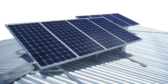
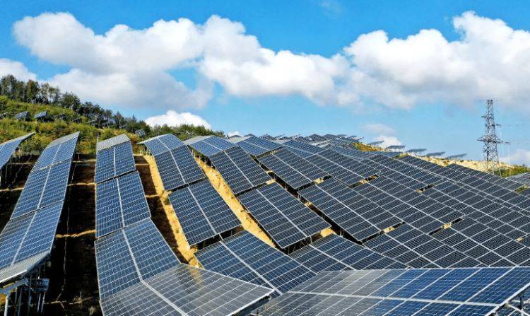
Photovoltaic (PV) power stands at the forefront of sustainable energy solutions, offering a renewable and abundant source of power. As the global energy landscape shifts towards cleaner alternatives, the significance of PV technology cannot be overstated. The optimization of PECVD (Plasma-Enhanced Chemical Vapor Deposition) processes within the PV industry is pivotal in this transition. By refining these processes, we can enhance the efficiency and durability of solar cells, thereby addressing pressing energy crises.
The role of PECVD in the manufacturing of crystalline silicon solar cells is particularly crucial. This technology is instrumental in the deposition of Si3N4 films, which play a key role in improving the optical properties and passivation of the cells. The quality of these films directly impacts the overall performance and longevity of the solar panels. Therefore, advancements in PECVD processes not only contribute to the technical efficiency of PV systems but also pave the way for broader adoption and integration of solar energy into the global energy mix.
Moreover, the economic implications of optimizing PECVD processes are substantial. By reducing the rework rate and minimizing defects, manufacturers can significantly cut down on production costs. This cost-effectiveness is essential for making solar energy competitive with traditional fossil fuel-based energy sources. As the demand for renewable energy continues to rise, the continuous improvement of PECVD techniques will be a cornerstone in meeting this escalating need.
In summary, the integration of advanced PECVD processes into PV technology is not merely a technical advancement but a strategic move towards a sustainable energy future. By enhancing the efficiency and reducing the costs of solar energy production, we can harness the full potential of photovoltaic power to address current and future energy challenges.
Related Products
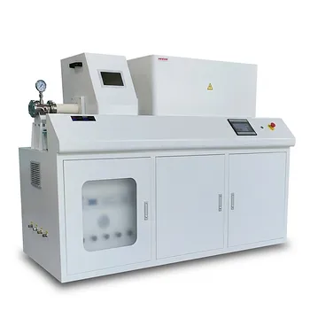
- Inclined Rotary Plasma Enhanced Chemical Vapor Deposition PECVD Equipment Tube Furnace Machine
- Chemical Vapor Deposition CVD Equipment System Chamber Slide PECVD Tube Furnace with Liquid Gasifier PECVD Machine
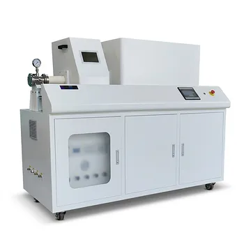
- Inclined Rotary Plasma Enhanced Chemical Vapor Deposition PECVD Equipment Tube Furnace Machine
- Custom CVD Diamond Coating for Lab Applications
- RF PECVD System Radio Frequency Plasma-Enhanced Chemical Vapor Deposition RF PECVD
Related Articles
- A Comprehensive Guide to PECVD Equipment Maintenance
- PECVD A Low-Cost and Scalable Method for 2D Material Preparation
- Plasma Enhanced Chemical Vapor Deposition (PECVD): A Comprehensive Guide
- PECVD Technology: Principles, Materials, Advantages, and Applications
- Understanding Glow Discharge in the PECVD Process
