Introduction to Diamond Thin Films
Properties and Applications of Diamond
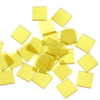
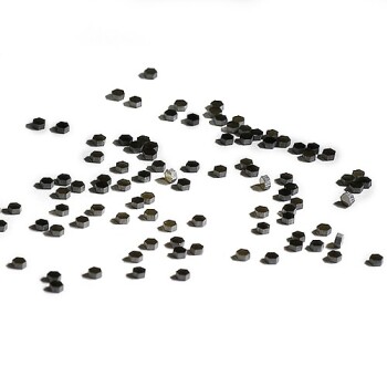
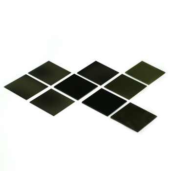
Diamond, renowned for its exceptional physical and chemical properties, finds extensive applications across multiple domains. Its unique characteristics make it indispensable in cutting tools, microelectromechanical systems (MEMS), biomedical devices, aerospace engineering, and nuclear energy sectors.
Mechanical Applications
One of the most significant properties of diamond is its unparalleled hardness, which is the highest among all known materials. This mechanical robustness makes diamond an ideal choice for wear-resistant coatings and cutting tools designed to machine hard materials. The low friction coefficient further enhances its utility in mechanical applications, reducing wear and tear and extending the lifespan of tools.
Optical Applications
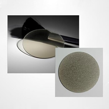
Diamond's optical transparency spans a broad range of the electromagnetic spectrum, from ultraviolet to infrared light. This property renders diamond suitable for use as transparent windows in specialized applications where conventional materials fall short. For instance, diamond windows are employed in environments where high transparency and resistance to extreme conditions are paramount, such as in high-pressure chambers or as components in optical instruments.
Electrical Applications
As a wide-bandgap semiconductor with a bandgap energy of 5.45 eV, diamond holds promising prospects in electronic devices and sensors. Its semiconductor properties enable the fabrication of high-power and high-frequency electronic components, which are crucial for next-generation technologies. Additionally, diamond's electrical insulation capabilities make it an excellent material for encapsulating sensitive electronic components, protecting them from electrical interference and damage.
Thermal Applications
Diamond boasts an exceptionally high thermal conductivity, ranging from 15 to 20 W/cm-K at ambient temperatures, which is approximately 20 times greater than that of copper. This superior heat dissipation capability positions diamond as a prime candidate for thermal management in miniaturized and high-performance electronic devices. Applications include heat sinks for lasers, transistors, and other heat-sensitive components, ensuring efficient cooling and prolonged operational life.
Environmental and Extreme Conditions
Diamond's outstanding chemical inertness and radiation hardness render it suitable for use in extreme environments. Whether it's high temperatures, radiation fields, or corrosive chemical environments, diamond's stability and durability make it a material of choice for components that must withstand harsh conditions. This property is particularly valuable in aerospace and nuclear energy sectors, where reliability under extreme conditions is critical.
Industrial Examples
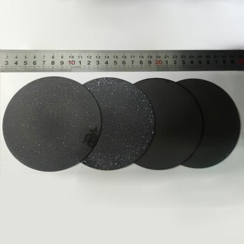
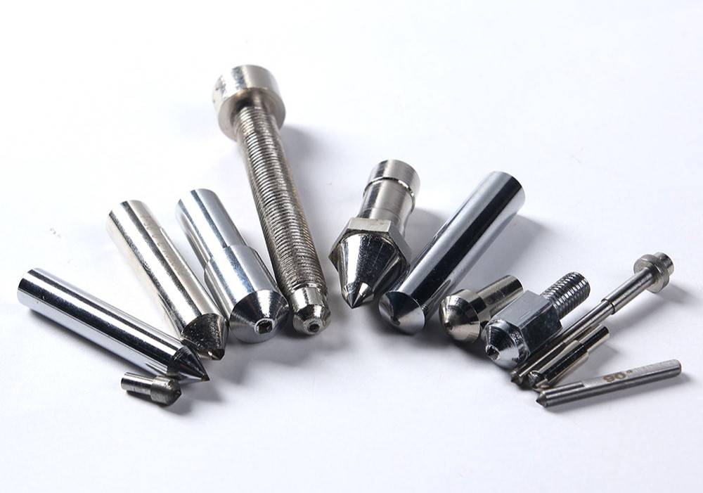
Several industrial applications exemplify the versatility of diamond. For instance, diamond-tipped tools are extensively used in machining and cutting applications, while diamond windows facilitate the transmission of infrared and microwave radiation. In the realm of electronics, diamond serves as a base material for semiconductor wafers and qubits in quantum computing, underscoring its pivotal role in advancing technological frontiers.
In summary, diamond's multifaceted properties not only enhance its value across traditional industries but also open new avenues for innovation in emerging technologies.
Challenges in Utilizing Natural Diamond
Natural diamonds present several significant challenges that hinder their widespread utilization despite their exceptional properties. The primary obstacles include their scarcity, high price, and limited size. These factors collectively limit the availability of natural diamonds for various industrial and technological applications.
The scarcity of natural diamonds is a direct result of their geological formation processes, which require specific high-temperature and high-pressure conditions over millions of years. This rarity translates into a high price that makes large-scale applications economically unfeasible. Additionally, the limited size of natural diamonds restricts their use in applications that require larger, continuous surfaces.
To convert graphite into diamond, high-temperature and high-pressure conditions are essential. This process, known as high-pressure high-temperature (HPHT) synthesis, mimics the natural geological conditions that form diamonds. However, creating these conditions in a controlled laboratory setting is both technically challenging and expensive. The need for specialized equipment and precise control over temperature and pressure adds to the complexity and cost of producing synthetic diamonds, further exacerbating the challenges associated with their utilization.
| Challenge | Description |
|---|---|
| Scarcity | Limited availability due to geological formation processes. |
| High Price | Resulting from rarity and the cost of extraction and processing. |
| Limited Size | Restricts use in applications requiring larger, continuous surfaces. |
| High-Temperature & High-Pressure | Essential for graphite to diamond conversion, adding to technical complexity and cost. |
These challenges underscore the need for alternative methods, such as Chemical Vapor Deposition (CVD), to produce diamond thin films more efficiently and cost-effectively.
Chemical Vapor Deposition (CVD) Methods
Historical Development of Diamond Synthesis
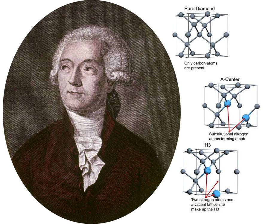
The quest for synthetic diamonds is a story that spans centuries, marked by significant milestones in the 20th century, particularly with the advent of Chemical Vapor Deposition (CVD) methods. The journey began with Antoine Lavoisier, a founding figure of modern chemistry, who discovered the similarity between a diamond's crystal lattice and carbon's crystal structure, laying the groundwork for early attempts to synthesize diamonds. This discovery, made in the late 18th century, was followed by numerous experiments to convert various forms of carbon into diamond, a process that required extreme conditions of temperature and pressure.
Early successes in diamond synthesis were reported by James Ballantyne Hannay in 1879 and Ferdinand Frédéric Henri Moissan in 1893. Hannay used a flame-heated tube, while Moissan employed his newly developed electric arc furnace, which involved striking an electric arc between carbon rods inside blocks of lime. Moissan's method, which involved rapid cooling of molten iron to generate the necessary high pressure, was documented in a series of articles in the 1890s.
The 20th century saw a significant shift with the introduction of CVD methods. In 1958, Union Carbide, led by Eversole, published a patent on low-pressure diamond synthesis, which was further developed by Angus, leading to a publication in 1968 on the growth of diamond seed crystals by vapor deposition. Around the same time, Spitsyn and Deryagin in Russia also developed a low-pressure diamond synthesis method, though its disclosure was delayed until 1980 due to security reasons.
High-Pressure High-Temperature (HPHT) synthesis dominated diamond fabrication until 1982 when breakthroughs in low-pressure CVD growth were published. The first significant paper on hot filament deposition by Matsumoto et al. in 1982 was followed by Kamo et al.'s work on "Diamond synthesis from gas in microwave plasma" in 1983. These publications ignited extensive research into low-pressure CVD diamond deposition, leading to the development of various types of synthetic diamonds, from ultra-pure and defect-free to conductive and quantum-grade diamonds.
Today, the synthesis of man-made diamonds has reached advanced levels, with applications spanning nearly every field, from cutting tools to quantum computing. The continuous refinement of CVD methods ensures that synthetic diamonds continue to close the gap with their natural counterparts, offering a sustainable and scalable solution to meet the growing demand for this remarkable material.
Common CVD Techniques
Chemical Vapor Deposition (CVD) techniques are pivotal in the synthesis of diamond thin films, each offering unique advantages and challenges. The most prevalent methods include:
-
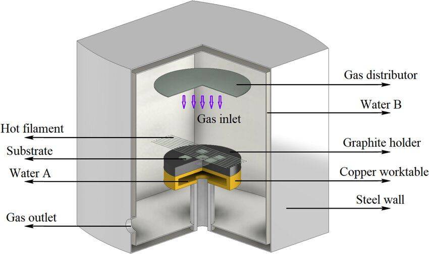
Hot Filament Chemical Vapor Deposition (HFCVD): Known for its simplicity and cost-effectiveness, HFCVD is widely used for preparing diamond tool coatings. However, it is susceptible to issues with oxidizing and corrosive gases, as well as metal contamination.
-
Microwave Plasma Chemical Vapor Deposition (MPCVD): This method excels in producing high-quality diamond films due to its stable discharge without electrodes. Despite this, challenges such as uneven plasma distribution and relatively low growth rates persist.
-
DC Plasma Chemical Vapor Deposition: Utilizing high-energy plasma, this technique achieves rapid growth rates. However, it is hampered by substantial equipment costs and difficulties in process control.
-
Combustion Flame Chemical Vapor Deposition: Ideal for atmospheric synthesis, Flame CVD offers a straightforward approach. Its limitations lie in the film area and quality, often compromised by thermal gradients and high gas consumption.
Each technique has its own set of advantages and drawbacks, making the choice of method crucial for optimizing the quality and application-specific properties of the resultant diamond films.
Hot Filament Chemical Vapor Deposition (HFCVD)
Hot Filament Chemical Vapor Deposition (HFCVD) stands out as a cost-effective and straightforward method for synthesizing diamond films, which are crucial for applications in cutting tools, microelectromechanical systems, and more. This technique involves the thermal dissociation of feed gases—typically a mixture of hydrogen (H₂) and methane (CH₄)—over a heated filament, typically made from refractory metals like tungsten (W), rhenium (Re), or tantalum (Ta). The filament, operating at temperatures ranging from 2173 to 2773 K, not only dissociates the carbon-containing precursor but also catalyzes the hydrogen dissociation, enhancing the overall process efficiency.
Despite its advantages, HFCVD is not without its challenges. One of the primary issues is the formation of metal carbides on the filament, which, while beneficial for catalyzing the reaction, leads to mechanical deterioration over time. This deterioration manifests as swelling, bending, cracking, and brittleness, ultimately compromising the filament's integrity and necessitating frequent replacements. Additionally, the close proximity of the filament to the substrate (typically 2-8 mm) can lead to metal contamination of the diamond film, a problem that remains difficult to mitigate.
| Advantages | Disadvantages |
|---|---|
| Cost-effective | Metal contamination |
| Simple setup | Filament deterioration |
| High growth rates | Oxidizing and corrosive gas issues |
The simplicity and rapid growth rates of HFCVD have made it a popular choice in diamond film research, but the ongoing challenges with filament durability and contamination highlight the need for continued innovation and optimization in the field.
Microwave Plasma Chemical Vapor Deposition (MPCVD)
Microwave Plasma Chemical Vapor Deposition (MPCVD) is a sophisticated method for synthesizing high-quality diamond films. This technique leverages microwave radiation to create a high-energy plasma within a reactor chamber, which is composed of a complex mixture of electrons, atomic ions, molecular ions, neutral atoms, molecules, and molecular fragments in various states. The electron density within this plasma is highest at the center, gradually diminishing as one moves outward. The primary mechanism for generating reactive gaseous precursors or fragments within the plasma is through electron impact dissociation.
The plasma produced by MPCVD is rich in reactive carbonaceous species and an excess of atomic or molecular hydrogen, which is essential for successful diamond deposition. These electrons absorb energy from the oscillating electric field of the microwave radiation, reaching temperatures as high as 5273 K, while the gas temperature (neutral species) remains relatively low, around 1073 K in low-pressure synthesis methods. The most commonly employed microwave frequencies for this process are 2.45 GHz and 915 MHz.
Despite its advantages, MPCVD is not without its challenges. One of the primary issues is the uneven distribution of plasma within the reactor chamber, which can lead to inconsistent diamond film quality. Additionally, the growth rates of diamond films produced via MPCVD are relatively low, which can be a limiting factor for industrial applications requiring large-scale production. Addressing these challenges requires a deeper understanding of the plasma dynamics and the optimization of process parameters to achieve more uniform and faster growth rates.

DC Plasma Chemical Vapor Deposition
DC Plasma Chemical Vapor Deposition (DC-PCVD) employs high-energy plasma to significantly enhance the growth rates of thin films. This method leverages a Direct Current (DC) electrical discharge to ionize and break down reacting gases, creating a highly reactive plasma environment. The high energy of the plasma not only accelerates the deposition process but also allows for the formation of complex compounds at lower temperatures compared to traditional thermal CVD methods.
However, the implementation of DC-PCVD is not without its challenges. The equipment required for this process is notably expensive, and maintaining precise control over the plasma conditions can be difficult. The complexity of the process stems from the need to balance the high-energy plasma with the stability of the deposition environment, ensuring uniform film growth and minimizing defects.
Despite these challenges, DC-PCVD offers unique advantages, particularly in the deposition of materials that require high reactivity and low thermal budgets. The ability to manipulate the plasma conditions allows for the deposition of a wide range of materials, including oxides, nitrides, and even alloys, opening up new possibilities for material science and industrial applications.
Flame Chemical Vapor Deposition
Flame Chemical Vapor Deposition (Flame CVD) stands out as a unique method within the Chemical Vapor Deposition (CVD) techniques due to its ability to facilitate atmospheric synthesis. This method leverages the combustion of gases to create a flame that serves as the reaction zone for depositing thin films. Despite its advantages, Flame CVD is not without its challenges. One of the primary limitations is the restricted film area that can be effectively covered. This limitation arises from the inherent thermal gradients present within the flame, which can lead to uneven deposition rates and non-uniform film thickness.
Moreover, the quality of the films produced through Flame CVD is often compromised due to these thermal gradients. The rapid consumption of gases in the flame also poses a significant constraint, as it can lead to inconsistent reactant concentrations, further affecting the film's quality. These factors collectively limit the applicability of Flame CVD in scenarios requiring large-area, high-quality thin films. Despite these drawbacks, Flame CVD remains a valuable technique for specific applications where atmospheric conditions and simplicity are paramount.
Factors Affecting Diamond Film Quality
Influence of Carbon Source Concentration
The concentration of methane, as the primary carbon source in Chemical Vapor Deposition (CVD) processes, plays a pivotal role in determining the morphology, structure, and overall quality of the diamond film. At suboptimal concentrations, the film may exhibit irregularities such as grainy textures or uneven thickness, which can compromise its mechanical and optical properties. Conversely, when the methane concentration is precisely tuned to the optimal range, the resulting diamond film demonstrates superior crystallinity, enhanced hardness, and improved thermal conductivity.
To illustrate the impact of methane concentration, consider the following table:
| Methane Concentration (%) | Film Morphology | Film Quality |
|---|---|---|
| 0.5 - 1.0 | Fine-grained, smooth | High |
| 1.0 - 2.0 | Medium-grained, uniform | Moderate |
| 2.0 - 3.0 | Coarse-grained, uneven | Low |
Optimal methane concentrations typically lie between 0.5% and 1.0%, where the balance between carbon supply and hydrogen etching is most favorable. Within this range, the hydrogen radicals effectively etch away non-diamond carbon phases, thereby stabilizing the diamond lattice and preventing the formation of graphitic structures. This etching process is crucial for maintaining the purity and integrity of the diamond film.
Moreover, the influence of methane concentration extends beyond the immediate film quality. It also affects the subsequent steps in the diamond growth process, such as nucleation density and the continuous growth of diamond clusters. A well-controlled methane concentration ensures that nucleation sites are evenly distributed, leading to a uniform film with minimal defects. Conversely, deviations from the optimal range can result in uneven nucleation, which may necessitate additional post-processing steps to rectify the film's structural integrity.
In summary, the meticulous control of methane concentration is indispensable for achieving high-quality diamond films through CVD processes. By fine-tuning this parameter, researchers and manufacturers can unlock the full potential of diamond thin films, paving the way for their application in cutting-edge technologies across various industries.
Effect of Nucleation Density
Nucleation density plays a pivotal role in determining the final characteristics of diamond thin films. Specifically, it significantly influences the surface morphology, grain size, and bonding force of the film. High nucleation density typically results in a finer grain structure, which can enhance the mechanical properties of the film, such as hardness and wear resistance. Conversely, lower nucleation densities may lead to larger grain sizes, which can compromise the film's uniformity and overall performance.
Impact on Surface Morphology
The surface morphology of the diamond film is directly correlated with nucleation density. A higher nucleation density tends to produce a smoother, more uniform surface, which is crucial for applications requiring precise surface finishes. For instance, in microelectromechanical systems (MEMS), a smooth surface is essential to ensure proper function and longevity. On the other hand, lower nucleation densities can result in a rougher surface, which may not meet the stringent requirements of certain applications.
Influence on Grain Size
Grain size is another critical parameter affected by nucleation density. As nucleation density increases, the average grain size decreases. This phenomenon is due to the higher number of nucleation sites competing for available carbon atoms during the growth process. Smaller grain sizes are generally desirable as they contribute to improved mechanical properties, such as increased hardness and reduced susceptibility to cracking.
Bonding Force Considerations
The bonding force between the diamond film and the substrate is also influenced by nucleation density. Higher nucleation densities can lead to stronger adhesion between the film and the substrate, which is essential for maintaining the film's integrity under mechanical stress. This strong bonding force is particularly important in applications where the diamond film is subjected to high mechanical loads, such as in cutting tools or wear-resistant coatings.
In summary, nucleation density is a fundamental factor in the preparation of high-quality diamond thin films. By carefully controlling nucleation density, researchers can optimize the surface morphology, grain size, and bonding force of the diamond film, thereby enhancing its performance in various industrial applications.
Substrate Material and Other Factors
The selection of substrate material and the pretreatment processes significantly influence the nucleation and subsequent growth of diamond films. Silicon and WC-Co (tungsten carbide-cobalt) substrates are commonly used, each presenting unique challenges and advantages.
Silicon Substrates
- Advantages: Silicon substrates are widely used due to their thermal stability and compatibility with semiconductor processing techniques. They provide a smooth surface for nucleation and growth, facilitating the formation of high-quality diamond films.
- Challenges: The thermal expansion mismatch between silicon and diamond can lead to stress and cracking during the deposition process. Additionally, silicon substrates require careful pretreatment to ensure uniform nucleation and minimize defects.
WC-Co Substrates
- Advantages: WC-Co substrates are preferred for their mechanical strength and wear resistance, making them suitable for applications in cutting tools and abrasives. The carbide component enhances the adhesion of diamond films.
- Challenges: The presence of cobalt in WC-Co substrates can lead to metal contamination, which affects the quality of the diamond film. Pretreatment processes, such as acid leaching, are necessary to remove cobalt and improve nucleation density.
Pretreatment Processes
- Surface Cleaning: Prior to deposition, substrates undergo rigorous cleaning to remove any contaminants, ensuring a clean surface for nucleation. Techniques include chemical etching and plasma cleaning.
- Surface Activation: Surface activation methods, such as argon or hydrogen plasma treatment, enhance the nucleation density by creating active sites on the substrate surface.
In summary, the choice of substrate material and the pretreatment processes are critical factors that determine the quality and performance of diamond films. Understanding these factors allows for the optimization of the CVD process, leading to improved diamond thin film applications.
Conclusion and Future Prospects
Current Challenges and Future Research
Despite significant advancements in the field of Chemical Vapor Deposition (CVD) for producing diamond thin films, several challenges persist, particularly in the quest for large-area single-crystal diamond films. These challenges are multifaceted, encompassing issues related to nucleation, growth mechanisms, and process optimization.
One of the primary hurdles lies in understanding and controlling the nucleation mechanisms. Nucleation is a critical phase in the formation of diamond films, dictating the initial crystal structure and subsequent growth. Current research indicates that the nucleation process is influenced by various factors, including the concentration of carbon sources, the presence of hydrogen radicals, and the nature of the substrate material. For instance, the concentration of methane in the gas phase significantly affects the morphology and structure of the diamond film. Optimal concentrations can lead to higher quality films, while suboptimal conditions can result in polycrystalline or defective structures.
Moreover, the role of hydrogen radicals in the CVD process cannot be overstated. These radicals play a crucial role in etching non-diamond carbon phases and stabilizing the diamond lattice, thereby preventing graphitization. However, achieving a stable and uniform distribution of hydrogen radicals remains a challenge, particularly in large-area deposition processes.
In addition to nucleation, optimizing process parameters is essential for enhancing the quality and scalability of diamond films. This involves fine-tuning variables such as temperature, pressure, and gas flow rates. For example, the Microwave Plasma Chemical Vapor Deposition (MPCVD) method, known for producing high-quality diamond films, faces challenges with uneven plasma distribution and low growth rates. Addressing these issues requires a deeper understanding of plasma dynamics and the development of advanced process control techniques.
Future research should therefore focus on several key areas:
- Nucleation Mechanisms: Investigating the underlying principles of nucleation to develop strategies for uniform and dense nucleation across large areas.
- Process Optimization: Refining CVD techniques to achieve stable and efficient growth conditions, particularly for large-scale production.
- Advanced Materials: Exploring new substrate materials and pretreatment processes that can enhance diamond nucleation and growth.
By addressing these challenges, the field of CVD diamond film synthesis can make substantial strides, paving the way for broader industrial applications and improved performance across various sectors.
The improved preparation methods of diamond thin films are poised to revolutionize these industries by offering solutions that were previously unattainable or impractical. As research continues to refine these techniques, the potential for even broader applications will undoubtedly expand, further solidifying diamond's role as a critical material in modern technology.
Related Products
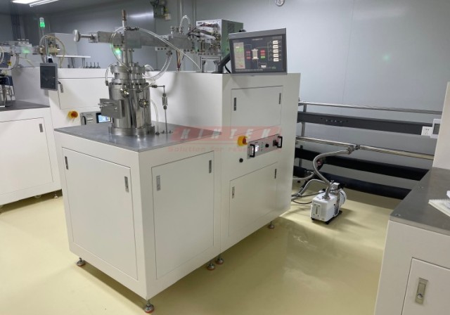
- HFCVD Machine System Equipment for Drawing Die Nano-Diamond Coating
- Custom CVD Diamond Coating for Lab Applications
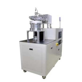
- Microwave Plasma Chemical Vapor Deposition MPCVD Machine System Reactor for Lab and Diamond Growth
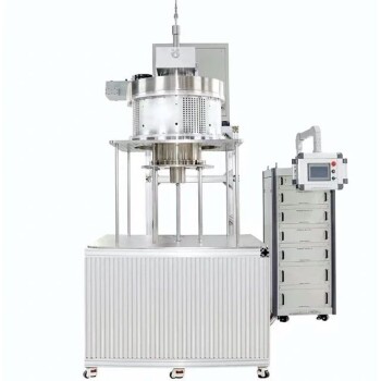
- 915MHz MPCVD Diamond Machine Microwave Plasma Chemical Vapor Deposition System Reactor
- Laboratory CVD Boron Doped Diamond Materials
