Introduce
As a high-performance fluoroplastic, polytetrafluoroethylene (PTFE) has become an indispensable key material in the semiconductor manufacturing field due to its unique chemical stability, corrosion resistance, high temperature resistance and excellent electrical insulation performance. From high-purity gas delivery pipelines to precision electrical insulation components, the multi-faceted application of PTFE in the semiconductor industry chain provides important guarantees for the purity, stability and reliability of the manufacturing process.
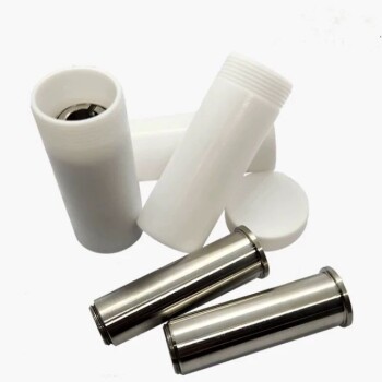
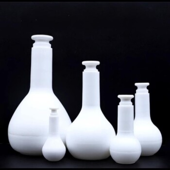
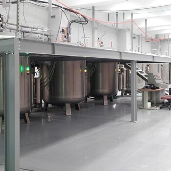
I. Core materials for gas and liquid delivery systems
Semiconductor manufacturing has extremely high requirements for the purity of gases and liquids. Even trace contamination may cause a significant drop in chip yield. PTFE and its modified materials (such as PFA) are ideal for conveying corrosive chemicals, high-purity gases and liquids due to their ultra-high chemical inertness and smooth surface properties:
- Corrosion resistance and high purity guarantee: PTFE hardly reacts with any chemical reagents (including strong acids, strong bases and organic solvents), which can effectively avoid contamination of the medium during the delivery process. For example, high-purity PFA tubes are used in semiconductor production to transport corrosive liquids such as etching solutions and cleaning agents. Their impurity-free release characteristics ensure the purity of process fluids.
- High-temperature environment adaptability: PTFE can maintain stable performance in a wide temperature range of -196°C to 260°C, meeting the transmission requirements of high-temperature gases (such as carrier gases in CVD processes) in semiconductor manufacturing. Its low permeability can also prevent gas leakage and ensure precise control of process parameters.
- Real-time monitoring advantages: The translucent PFA tube design allows engineers to directly observe the state of the fluid in the tube, quickly identify bubbles or contaminants, and significantly improve the efficiency of handling process abnormalities.
II. The ultimate application of electrical insulation performance
Semiconductor equipment involves high-frequency signal transmission and precision circuit systems, and the requirements for insulating materials are extremely stringent. PTFE's dielectric properties make it the material of choice for key electrical components:
- High-frequency signal integrity: PTFE's low dielectric constant (about 2.1) and low loss factor remain stable in the 60-600 billion Hz range, making it an ideal insulating medium for 5G communication equipment, high-frequency chip packaging and other scenarios, minimizing signal attenuation.
- Extreme environmental reliability: PTFE can still maintain high insulation resistance (>10^18 Ω·cm) and breakdown strength (>20 kV/mm) in high temperature, high humidity or strong electromagnetic interference environments. For example, the insulation layer of the heating element of semiconductor equipment uses modified PTFE, which can work for a long time at more than 200°C without failure.
- Electrostatic protection function: PTFE's low friction coefficient (0.05-0.1) can effectively inhibit static electricity accumulation and prevent microstructural damage caused by electrostatic discharge during wafer processing.
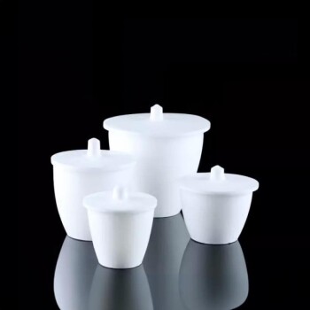
III. Pollution control and process stability improvement
The cleanliness requirement for semiconductor manufacturing is ISO Class 1 (≤12 particles per cubic meter). PTFE's multiple characteristics provide multiple guarantees for the clean room environment:
- Surface anti-stick properties: PTFE's ultra-low surface energy makes it almost non-adhesive to any substance. When used for reaction chamber linings and wafer carrier coatings, it can significantly reduce byproduct deposition and extend equipment maintenance cycles.
- Chemical inertness protection: In wet cleaning, etching and other processes, valve seals and pump body parts made of PTFE can withstand long-term erosion by highly corrosive reagents such as hydrofluoric acid and ammonia, avoiding metal ion contamination.
- Precision component manufacturing: Through injection molding or powder metallurgy processes, PTFE can be processed into nano-precision fixtures, pipe connectors, etc., to meet the assembly requirements of high-precision equipment such as lithography machines.
IV. Frontier Applications and Technical Challenges
As semiconductor processes move toward nodes below 3nm, PTFE materials are also continuing to innovate:
- Nano-filling modification: By adding carbon nanotubes or graphene, the thermal conductivity and mechanical strength of PTFE are improved, making it suitable for the heat dissipation insulation layer of high-power chips.
- Ultra-thin coating technology: Nano-scale PTFE coatings prepared by atomic layer deposition (ALD) have been used for anti-pollution protection of extreme ultraviolet lithography (EUV) optical components.
- Environmental recycling problems: Although the chemical stability of PTFE brings advantages in use, its difficult degradation characteristics also cause environmental concerns. The industry is currently exploring chemical depolymerization and recycling technology.
Conclusion
From gas pipelines to electrical insulation, the role of PTFE in semiconductor manufacturing has penetrated into the entire industry chain, including wafer manufacturing, packaging testing, and equipment maintenance. With the rapid development of third-generation semiconductor materials, the performance requirements for PTFE will become more stringent. In the future, through breakthroughs in molecular structure optimization, composite material development and green manufacturing technology, PTFE is expected to play a more critical role in emerging fields such as quantum computing chips and silicon carbide power devices. The continuous innovation of this material will become an important cornerstone for promoting the advancement of semiconductor technology.
CONTACT US FOR A FREE CONSULTATION
KINTEK LAB SOLUTION's products and services have been recognized by customers around the world. Our staff will be happy to assist with any inquiry you might have. Contact us for a free consultation and talk to a product specialist to find the most suitable solution for your application needs!