In the world of electronics, semiconductors are defined by their extreme thinness. While the silicon wafer they are built upon has a tangible thickness for structural integrity, the active, functional layers of a semiconductor are measured in nanometers—a scale thousands of times thinner than a human hair. The final product you see, the chip, is a small, thin package designed for a specific purpose.
The immense power of a semiconductor comes not from its bulk, but from the microscopic thinness of its functional layers. This thinness is a deliberate engineering choice that allows for the speed, efficiency, and density that define modern computing.
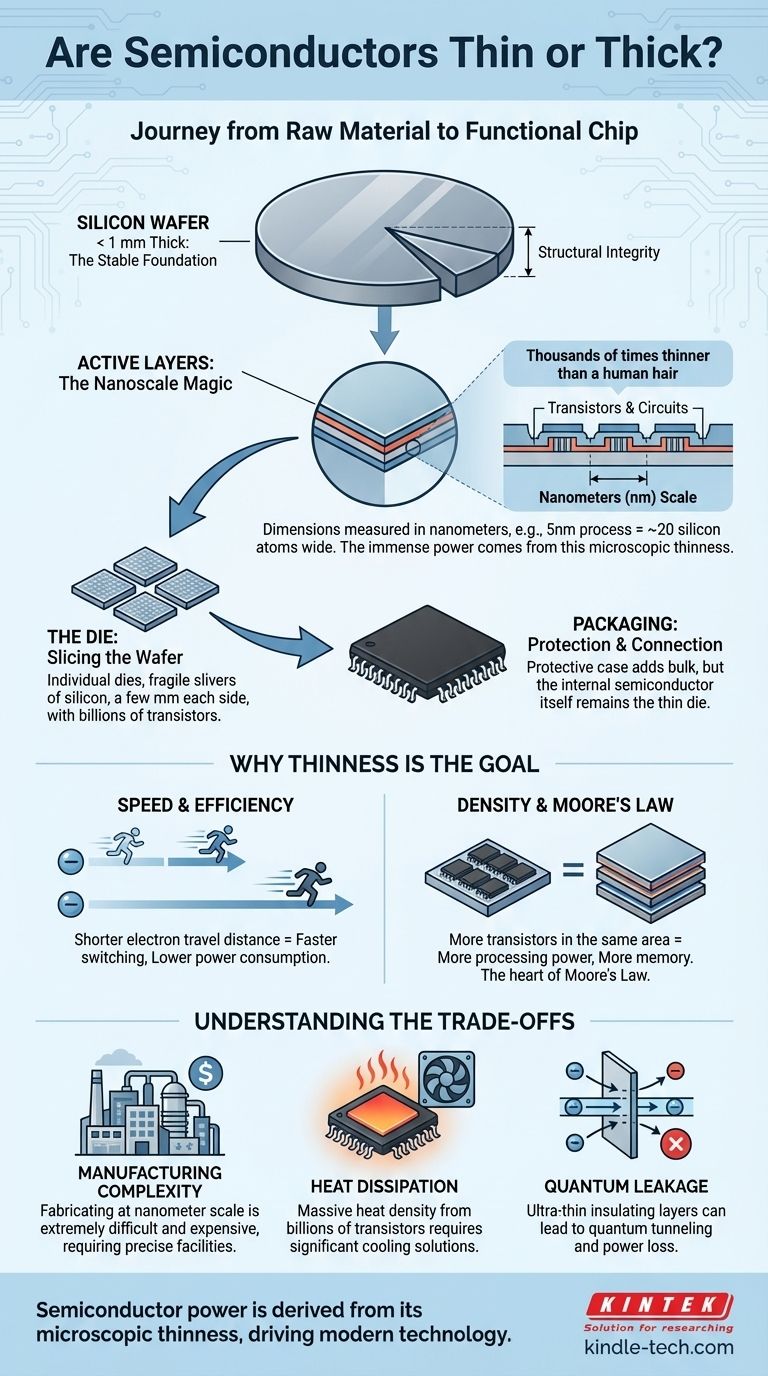
From Raw Material to Functional Chip
To understand the dimension of a semiconductor, we must look at its journey from a raw silicon wafer to a packaged chip. The process involves both relatively "thick" and unbelievably "thin" components.
The Silicon Wafer: A Stable Foundation
A semiconductor device begins its life as a part of a silicon wafer. This is a highly pure, perfectly flat, and rigid disc that acts as the substrate, or foundation, for building circuits.
A typical wafer might be 300mm (about 12 inches) in diameter and less than 1mm thick. This thickness is crucial for providing the mechanical stability needed to handle the wafer during the complex manufacturing process without it breaking.
The Active Layers: Where the Magic Happens
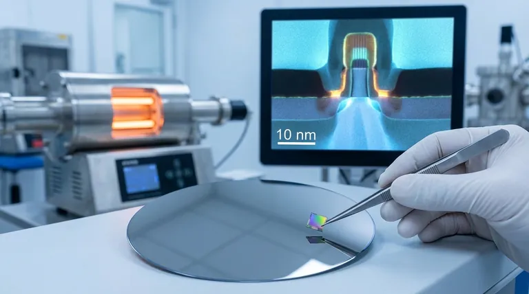
The actual work of a semiconductor is performed in transistors and circuits built on top of the wafer. These are created by depositing and etching a series of incredibly thin films of various materials.
These active layers are where the term "thin" becomes an understatement. Their dimensions are measured in nanometers (nm). For context, a 5nm manufacturing process refers to features on the chip that are only about 20 silicon atoms wide.
The Die: Slicing the Wafer
A single wafer contains hundreds or even thousands of identical, individual circuits. The wafer is precisely cut, or diced, into these individual rectangular units. Each unit is called a die.
A single die is a fragile, tiny sliver of silicon, often just a few millimeters on each side, containing billions of transistors in its nanometer-scale layers.
Packaging: Protection and Connection
The bare silicon die is too fragile to be used directly. It is placed into a protective package, which is typically the black plastic or ceramic component we recognize as a "chip."
This package serves two critical roles: it protects the delicate die from the environment and provides the metal pins or pads needed to connect the chip to a larger circuit board. The package adds bulk and thickness, but the semiconductor itself remains the thin die inside.
Why Thinness Is the Ultimate Goal
Semiconductor engineers are in a constant race to make the functional layers of a chip thinner and smaller. This obsession with thinness is directly tied to performance.
Speed and Efficiency
The speed of a transistor is determined by how quickly it can switch on and off. In thinner, smaller transistors, electrons have a much shorter distance to travel.
This directly translates to faster switching speeds and lower power consumption, similar to how a shorter sprint requires less time and energy than a long run.
Density and Moore's Law
Thinner layers and smaller components allow engineers to pack more transistors into the same physical area. This principle is the heart of Moore's Law.
More transistors per chip mean more processing power, more memory, and more advanced features, all within a device of the same size.
Understanding the Trade-offs
Pursuing microscopic thinness is not without its challenges. The benefits in performance come with significant engineering and physical trade-offs.
Manufacturing Complexity
Fabricating nanometer-scale layers is extraordinarily difficult and expensive. It requires multi-billion dollar facilities known as "fabs" and some of the most precise manufacturing processes ever developed by humanity.
Heat Dissipation
While smaller transistors are more efficient individually, packing billions of them into a tiny space creates a massive heat density problem. The "thin" die generates so much heat that it often requires a "thick" cooling solution, like a heat sink or fan, to operate without damage.
Quantum Leakage
As insulating layers become just a few atoms thick, a quantum mechanical effect called tunneling becomes a serious problem. Electrons can "leak" through these ultra-thin barriers, wasting power and causing computational errors. This is a fundamental physical limit that engineers are constantly battling.
Making the Right Choice for Your Goal
Your perspective on a semiconductor's thickness depends entirely on your role and what you need to achieve.
- If your primary focus is hardware design: You must balance the performance gains from smaller, thinner transistors against the critical need for thermal management and power integrity.
- If your primary focus is software development: You can leverage the speed of modern "thin" hardware, but be aware that performance can be throttled by the physical limits of heat dissipation on the chip.
- If your primary focus is business or investment: You should view the pursuit of "thinness" (advances in process nodes) as the primary engine of technological progress, but recognize the immense capital costs and physical barriers involved.
Understanding that a semiconductor's power is derived from its microscopic thinness provides the fundamental context for nearly all of modern technology.
Summary Table:
| Component | Typical Thickness | Purpose |
|---|---|---|
| Silicon Wafer | < 1 mm | Provides structural foundation |
| Active Layers | Nanometers (nm) | Functional circuits and transistors |
| Die (Chip) | A few mm (side length) | Individual circuit unit |
| Final Package | Varies (chip casing) | Protection and external connection |
Unlock Precision for Your Lab with KINTEK
Harnessing the power of thin-film technology is at the heart of modern semiconductor innovation. At KINTEK, we specialize in providing high-quality lab equipment and consumables that support the precise fabrication and analysis of these microscopic layers. Whether you are involved in materials research, semiconductor development, or electronics testing, our solutions are designed to meet the rigorous demands of your work.
Why Choose KINTEK?
- Precision Tools: From deposition systems to etching equipment, we offer reliable tools for creating and handling nanometer-scale layers.
- Expert Support: Our team understands the challenges of semiconductor manufacturing and is here to help you optimize your processes.
- Tailored Solutions: We serve laboratories and R&D teams focused on advancing technology through cutting-edge thin-film applications.
Ready to enhance your capabilities in semiconductor research or production? Contact us today to discuss how KINTEK can support your laboratory needs and help you achieve breakthrough results.
Visual Guide
Related Products
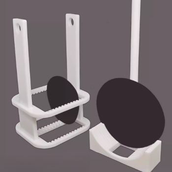
- Customizable PTFE Wafer Carriers for Semiconductor and Lab Applications
- Boron Nitride (BN) Ceramic Plate
- Silicon Carbide (SIC) Ceramic Sheet Wear-Resistant Engineering Advanced Fine Ceramics
- Thin-Layer Spectral Electrolysis Electrochemical Cell
- Reference Electrode Calomel Silver Chloride Mercury Sulfate for Laboratory Use
People Also Ask
- What are the technical advantages of using PTFE laboratory consumables? Ensure Ultimate Chemical Resistance
- Why is slender PTFE tubing necessary for flow control in multi-channel catalyst aging? Ensure Equal Gas Distribution
- Is PTFE corrosion resistant? Discover the Ultimate Chemical Resistance for Your Lab
- What is the function of a customized PTFE cap in IL-TEM? Bridge the Gap Between Microscopy and Electrochemistry
- Why are PTFE containers required for PCT leaching tests? Ensure Chemical Inertness and Analytical Precision