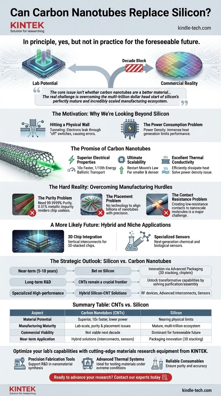
In principle, yes, but not in practice for the foreseeable future. While carbon nanotubes (CNTs) possess electrical properties far superior to silicon and have been used to build working processors in lab settings, they face monumental manufacturing and purity challenges. These obstacles make it commercially unviable for CNTs to replace silicon as the foundation of the global semiconductor industry within the next decade.
The core issue isn't whether carbon nanotubes are a better material for transistors—at the nanoscale, they are. The real challenge is overcoming the multi-trillion dollar head start of silicon's perfectly mature and incredibly scaled manufacturing ecosystem.
The Motivation: Why We're Looking Beyond Silicon
For decades, the tech industry has been powered by Moore's Law—the predictable doubling of transistors on a chip every two years. This progress has been achieved by relentlessly shrinking silicon transistors. However, we are now approaching the fundamental physical limits of this process.
Hitting a Physical Wall
As silicon components shrink to just a few nanometers, a quantum mechanical effect called tunneling becomes a serious problem. Electrons can leak through the transistor's "off" switch, or gate, causing errors and wasting power. This makes further scaling increasingly difficult and less effective.
The Power Consumption Problem
Even before we hit the absolute physical limit, heat becomes the primary bottleneck. Packing more silicon transistors into a small area generates immense heat. This power density issue limits chip performance far more than our ability to physically etch smaller components.
The Promise of Carbon Nanotubes
Carbon nanotubes are cylindrical molecules of carbon atoms that are incredibly small—as narrow as one nanometer in diameter. They represent one of the most promising candidates for post-silicon electronics.
Superior Electrical Properties
CNTs can conduct electricity with almost no resistance, a property known as ballistic transport. This means electrons can fly through them without scattering, enabling transistors that are potentially 10 times faster and use one-tenth the energy of their silicon counterparts.
Ultimate Scalability
Because of their minuscule size, CNTs could theoretically be used to build transistors and processors far smaller and more densely packed than anything achievable with silicon. This could restart the engine of Moore's Law.
Excellent Thermal Conductivity
CNTs are also exceptional thermal conductors. Their ability to efficiently dissipate heat is a crucial advantage that could help solve the power density problem plaguing high-performance silicon chips.
The Hard Reality: Overcoming Manufacturing Hurdles
Despite their theoretical perfection, the path from a lab demonstration to a billion-transistor commercial chip is blocked by immense, practical challenges.
The Purity Problem
CNTs can form in two types: semiconducting (which can be switched on and off) and metallic (which are always on). For a processor, you need billions of purely semiconducting CNTs. Even a 0.01% metallic impurity in the mix can cause short circuits and render a chip useless. Achieving 99.9999% purity at an industrial scale remains an unsolved problem.
The Placement Problem
Modern chips are built with near-atomic precision. Silicon manufacturing allows for the perfect placement of billions of components. There is currently no technology that can place and align billions of individual carbon nanotubes on a wafer with the required density and perfection.
The Contact Resistance Problem
A transistor is useless if you can't get electricity into and out of it efficiently. Creating a low-resistance electrical contact to a molecule that is only a nanometer wide is a profound engineering challenge. High contact resistance can easily negate the intrinsic performance benefits of the CNT itself.
A More Likely Future: Hybrid and Niche Applications
Instead of a complete replacement, the most probable future involves CNTs augmenting silicon in specialized ways. This hybrid approach leverages the best of both worlds: silicon's mature fabrication and CNTs' unique properties.
3D Chip Integration
One of the most promising near-term applications is using CNTs as vertical interconnects in 3D-stacked chips. As chipmakers stack layers of silicon to increase density, the wires connecting them become a major bottleneck. The superior conductivity of CNTs makes them an ideal material for these connections.
Specialized Sensors
CNTs have an extremely high surface-area-to-volume ratio, making them incredibly sensitive to their environment. This makes them perfect for next-generation chemical and biological sensors, an application where mass-manufacturing hurdles are less critical than unique performance.
The Strategic Outlook: Silicon vs. Carbon Nanotubes
Understanding the state of these materials requires separating theoretical potential from commercial reality.
- If your primary focus is near-term commercial computing (next 5-10 years): Bet on silicon. Innovation will come from advanced packaging like 3D stacking and chiplets, not a fundamental material change.
- If your primary focus is long-term R&D or advanced materials: CNTs remain a crucial frontier for post-silicon electronics, where solving the challenges of purification and directed assembly could unlock transformative capabilities.
- If your primary focus is specialized, high-performance applications: Watch for hybrid silicon-CNT solutions to emerge first, likely in areas like radio-frequency (RF) devices, advanced interconnects, or highly sensitive sensors.
The ultimate path forward in computing depends on mastering manufacturing at the atomic scale.
Summary Table:
| Aspect | Carbon Nanotubes (CNTs) | Silicon |
|---|---|---|
| Material Potential | Superior ballistic transport, 10x faster, lower power | Nearing fundamental physical limits |
| Manufacturing Maturity | Lab-scale; purity and placement challenges | Perfectly mature, multi-trillion dollar ecosystem |
| Commercial Viability | Not viable for the next decade | Dominant for foreseeable future |
| Near-term Application | Hybrid solutions (interconnects, sensors) | Continued innovation in packaging and 3D stacking |
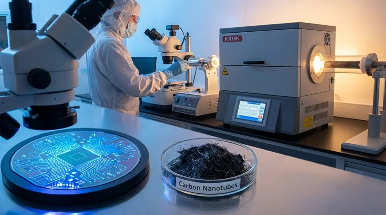
Optimize your lab's capabilities with cutting-edge materials research equipment from KINTEK.
As the semiconductor industry pushes the boundaries of Moore's Law, having the right tools for advanced materials research is crucial. Whether you are exploring carbon nanotubes, silicon alternatives, or hybrid solutions, KINTEK provides the high-precision lab equipment and consumables you need to drive innovation.
- Precision Fabrication Tools: Support your R&D in nanomaterial synthesis and characterization.
- Advanced Thermal Systems: Ideal for testing materials under extreme conditions.
- Reliable Consumables: Ensure purity and accuracy in every experiment.
Ready to advance your research? Contact our experts today to discuss how KINTEK's solutions can accelerate your development of next-generation electronics.
Visual Guide
Related Products
- Carbon Graphite Boat -Laboratory Tube Furnace with Cover
- Boron Nitride (BN) Ceramic Tube
- Hexagonal Boron Nitride HBN Thermocouple Protection Tube
People Also Ask
- Why is graphite used in furnaces? For Extreme Heat, Purity, and Efficiency
- What is the use of graphite furnace? Achieve Extreme-Temperature Processing for Advanced Materials
- What is the technical value of using graphite crucibles with graphite paper liners? Optimize Zr3(Al1-xSi)C2 Synthesis
- What metals can you melt in a graphite crucible? A Guide to Safe & Efficient Melting
- What is the disadvantage of graphite furnace? Managing Reactivity and Contamination Risks