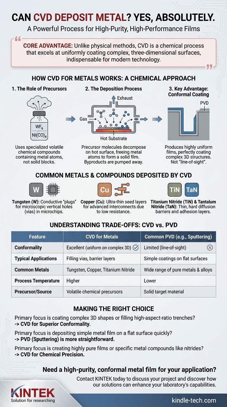
Yes, absolutely. While Chemical Vapor Deposition (CVD) is famously used for depositing semiconductor materials like polysilicon, it is also a powerful and widely utilized industrial process for depositing high-purity, high-performance films of pure metals and metallic compounds. The technique's unique advantages make it essential for advanced applications, particularly in microelectronics.
The core advantage of using CVD for metals is not just that it can be done, but how it's done. Unlike physical methods, CVD is a chemical process that excels at uniformly coating complex, three-dimensional surfaces, making it indispensable for modern technology.
How CVD for Metals Works: A Chemical Approach
The Role of Precursors
CVD does not use a solid block of metal as its source. Instead, it uses a volatile precursor—a specialized chemical compound that contains the metal atoms you want to deposit.
These precursors are often gases or liquids with a high vapor pressure. Common examples include metal halides (like tungsten hexafluoride, WF₆), metal carbonyls (like nickel carbonyl, Ni(CO)₄), and various organometallic compounds.
The Deposition Process
The process is a controlled chemical reaction. The metal precursor gas is introduced into a reaction chamber containing the object to be coated, known as the substrate, which is heated to a specific temperature.
On the hot surface, the precursor molecules decompose or react with other gases. This reaction breaks the chemical bonds, freeing the metal atoms, which then deposit onto the substrate to form a solid film. The remaining parts of the precursor molecule (the byproducts) are pumped away as waste gas.
Key Advantage: Conformal Coating
Because the deposition happens from a gas phase that surrounds the substrate, CVD is not a "line-of-sight" process. This allows it to produce highly conformal films.
A conformal film has a uniform thickness, perfectly coating every surface, including the bottom and sidewalls of deep trenches or complex 3D structures. This is a critical capability where physical deposition methods often fail.
Common Metals and Compounds Deposited by CVD
While many metals can be deposited via CVD, a few are cornerstones of the semiconductor industry.
Tungsten (W)
Tungsten is one of the most common metals deposited by CVD. It is used to create conductive "plugs" that fill microscopic vertical holes (vias) to connect different layers of circuitry in a microchip. Its ability to perfectly fill these high-aspect-ratio features is a textbook example of CVD's power.
Copper (Cu)
Copper replaced aluminum as the primary interconnect material in advanced microchips due to its lower electrical resistance. CVD (and a related technique, ALD) is used to deposit ultra-thin, conformal copper seed layers before the bulk of the copper is filled in by another process.
Metal Compounds: Barriers and Adhesion Layers
Often, the goal isn't a pure metal but a specific metallic compound. CVD is exceptionally good at this.
Titanium Nitride (TiN) and Tantalum Nitride (TaN) are deposited as incredibly thin diffusion barriers. These layers prevent metals like copper from migrating into the surrounding silicon, which would destroy the device. These nitride films are hard, chemically stable, and conductive.
Understanding the Trade-offs: CVD vs. PVD
CVD is not the only way to deposit thin films. It is often compared to Physical Vapor Deposition (PVD), which includes techniques like sputtering and evaporation.
Film Quality and Conformality
CVD typically produces films with higher purity, better density, and vastly superior conformality compared to PVD. If you need to coat a complex shape uniformly, CVD is often the only viable option.
Process Complexity and Safety
CVD processes can be more complex and expensive. They require higher temperatures and involve precursor chemicals and byproducts that can be highly toxic, corrosive, or flammable, demanding sophisticated safety and handling protocols.
Material Availability
PVD is more versatile for depositing a wide range of pure elements and alloys, as you can simply use a solid target of that material. CVD is limited by the availability of a suitable volatile precursor, and developing a new CVD process for a new material can be a significant research and development effort.
Making the Right Choice for Your Goal
Deciding between CVD and other methods depends entirely on the technical requirements of your application.
- If your primary focus is coating complex 3D shapes or filling high-aspect-ratio trenches: CVD is the superior choice due to its unmatched conformality.
- If your primary focus is depositing a simple metal film on a flat surface quickly and at lower temperatures: PVD techniques like sputtering are often more straightforward and cost-effective.
- If your primary focus is creating highly pure films or specific metal compounds like nitrides for barrier layers: CVD provides the chemical precision needed to achieve the desired film structure and properties.
Ultimately, your choice is dictated by whether your priority is the geometric challenge of conformality or the material simplicity of physical deposition.
Summary Table:
| Feature | CVD for Metals | Common PVD (e.g., Sputtering) |
|---|---|---|
| Conformality | Excellent (uniform on complex 3D shapes) | Limited (line-of-sight) |
| Typical Applications | Filling vias, barrier layers (TiN, TaN) | Simple coatings on flat surfaces |
| Common Metals | Tungsten (W), Copper (Cu), Titanium Nitride (TiN) | Wide range of pure metals and alloys |
| Process Temperature | Higher | Lower |
| Precursor/Source | Volatile chemical precursors | Solid target material |
Need a high-purity, conformal metal film for your application?
Choosing the right deposition technology is critical for your project's success. The experts at KINTEK specialize in advanced lab equipment, including CVD and PVD systems, to meet your specific research and production needs for microelectronics, semiconductors, and advanced materials.
We can help you determine if CVD is the right solution for your metal deposition challenges, ensuring superior film quality and performance.
Contact KINTEK today to discuss your project and discover how our solutions can enhance your laboratory's capabilities.
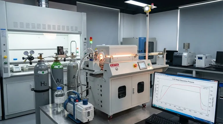
Visual Guide
Related Products
- CVD Diamond Dressing Tools for Precision Applications
- Multi Heating Zones CVD Tube Furnace Machine Chemical Vapor Deposition Chamber System Equipment
- CVD Diamond Domes for Industrial and Scientific Applications
- CVD Diamond for Thermal Management Applications
- Chemical Vapor Deposition CVD Equipment System Chamber Slide PECVD Tube Furnace with Liquid Gasifier PECVD Machine
People Also Ask
- What is chemical vapor deposition of diamond? Grow High-Purity Diamonds Atom-by-Atom
- How long does it take to make synthetic diamonds? Discover the 6-8 Week Science Behind Lab-Grown Gems
- Can CVD diamonds change color? No, their color is permanent and stable.
- What is CVD diamond? The Ultimate Guide to Lab-Grown Diamonds and Their Uses
- What are the disadvantages of CVD diamonds? Understanding the trade-offs for your purchase.


