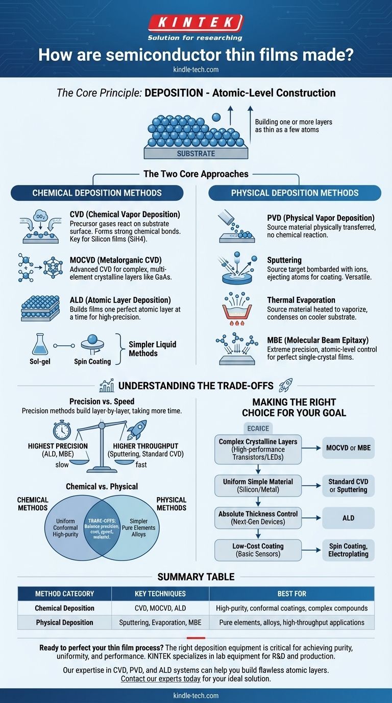
At its core, creating a semiconductor thin film is an act of controlled construction at the atomic level. These films are made using deposition, a process where material is carefully transferred onto a base, or substrate, to build one or more layers that can be as thin as a few atoms. The two primary families of techniques used to achieve this are Chemical Vapor Deposition (CVD) and Physical Vapor Deposition (PVD).
The fundamental challenge of making a semiconductor thin film is not just about creating a thin layer; it's about flawlessly arranging atoms to build a perfect, ultra-pure structure. The choice of manufacturing method is therefore dictated by the specific material, the required purity, and the complexity of the atomic structure needed for the final device.
The Fundamental Principle: Deposition
What is Deposition?
Deposition is the controlled synthesis of a material as a thin film. Think of it as painting with individual atoms or molecules.
The goal is to build a layer, or multiple layers, on a substrate with precise control over its thickness, chemical composition, and physical structure.
Why is it the Core Concept?
The properties of a semiconductor device—from a computer chip's transistor to a solar panel's light-absorbing layer—are defined by the quality of its thin films.
Even a few misplaced atoms or a minor impurity can create a defect that completely compromises the device's performance. Therefore, the entire manufacturing process is optimized for perfect, repeatable deposition.
The Two Core Approaches: Chemical vs. Physical
Nearly all advanced manufacturing techniques fall into two categories, distinguished by how they move material onto the substrate.
Chemical Deposition Methods
In chemical methods, precursor gases or liquids react on the substrate's surface, leaving behind the desired solid material.
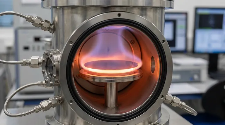
Chemical Vapor Deposition (CVD) is a cornerstone technique. Precursor gases, such as silane (SiH4) for silicon films, are introduced into a reactor where they decompose and deposit atoms onto the substrate, forming strong chemical bonds.
For more complex, multi-element crystalline layers like gallium arsenide, a more advanced version called Metalorganic CVD (MOCVD) is used.
Other chemical methods include Atomic Layer Deposition (ALD), which builds films one perfect atomic layer at a time, and simpler liquid-based techniques like sol-gel or spin coating for less demanding applications.
Physical Deposition Methods
In physical methods, the source material is physically displaced and transferred to the substrate without a chemical reaction.
Physical Vapor Deposition (PVD) is a broad category that includes several key techniques.
One common method is sputtering, where a source target is bombarded with high-energy ions, knocking atoms loose that then travel and coat the substrate.
Another is thermal evaporation, where the source material (often in pellet or granule form) is heated in a vacuum until it vaporizes. These vaporized atoms then travel in a straight line and condense on the cooler substrate, forming the film.
More sophisticated methods like Molecular Beam Epitaxy (MBE) offer extreme precision, depositing material with atomic-level control to grow perfect single-crystal films.
Understanding the Trade-offs
No single method is universally superior. The choice involves balancing precision, cost, speed, and the specific material requirements.
Chemical vs. Physical
Chemical methods like CVD excel at creating uniform, chemically bonded films that conform well to complex surface topographies. They are ideal for producing high-purity compound semiconductors.
Physical methods like sputtering are often simpler and more versatile for depositing pure elements and alloys. However, they can be less effective at coating intricate, non-flat surfaces.
Precision vs. Speed
Techniques offering the highest precision, such as Atomic Layer Deposition (ALD) and Molecular Beam Epitaxy (MBE), are inherently slow because they build the film one atomic layer at a time.
Higher-throughput methods like sputtering or standard CVD are faster and more economical for applications where atomic-level perfection is not the absolute priority. The final choice always depends on the performance requirements of the electronic device.
Making the Right Choice for Your Goal
Your application's specific needs will dictate the ideal deposition strategy.
- If your primary focus is creating complex, high-purity crystalline layers for high-performance transistors or LEDs: MOCVD or MBE are the industry standards for achieving the necessary structural perfection.
- If your primary focus is depositing a uniform layer of a simple material like silicon or a metal: Standard CVD or a PVD method like sputtering offers a reliable balance of quality and manufacturing efficiency.
- If your primary focus is absolute control over thickness with atomic-level precision for next-generation devices: ALD is the superior choice, providing unparalleled conformity and control, one layer at a time.
- If your primary focus is a low-cost coating for less critical applications like basic sensors or protective layers: Simpler liquid-based methods like spin coating or even electroplating may be sufficient.
Mastering the deposition of thin films is the foundational skill that enables the entire modern electronics industry.
Summary Table:
| Method Category | Key Techniques | Best For |
|---|---|---|
| Chemical Deposition | CVD, MOCVD, ALD | High-purity, conformal coatings, complex compounds |
| Physical Deposition | Sputtering, Evaporation, MBE | Pure elements, alloys, high-throughput applications |
Ready to perfect your thin film process? The right deposition equipment is critical for achieving the purity, uniformity, and performance your semiconductor applications demand. KINTEK specializes in lab equipment and consumables, serving the precise needs of R&D and production laboratories. Our expertise in CVD, PVD, and ALD systems can help you build flawless atomic layers. Contact our experts today to discuss your specific requirements and find the ideal solution for your lab.
Visual Guide
Related Products
- Chemical Vapor Deposition CVD Equipment System Chamber Slide PECVD Tube Furnace with Liquid Gasifier PECVD Machine
- RF PECVD System Radio Frequency Plasma-Enhanced Chemical Vapor Deposition RF PECVD
- Microwave Plasma Chemical Vapor Deposition MPCVD Machine System Reactor for Lab and Diamond Growth
- Customer Made Versatile CVD Tube Furnace Chemical Vapor Deposition Chamber System Equipment
- 915MHz MPCVD Diamond Machine Microwave Plasma Chemical Vapor Deposition System Reactor
People Also Ask
- Why is Chemical Vapor Deposition (CVD) equipment uniquely suited for constructing hierarchical superhydrophobic structures?
- What is the chemical vapor deposition growth process? Build Superior Thin Films from the Atom Up
- What are the processes of vapor phase deposition? Understand CVD vs. PVD for Superior Thin Films
- What happens during deposition chemistry? Building Thin Films from Gaseous Precursors
- How expensive is chemical vapor deposition? Understanding the True Cost of High-Performance Coating


