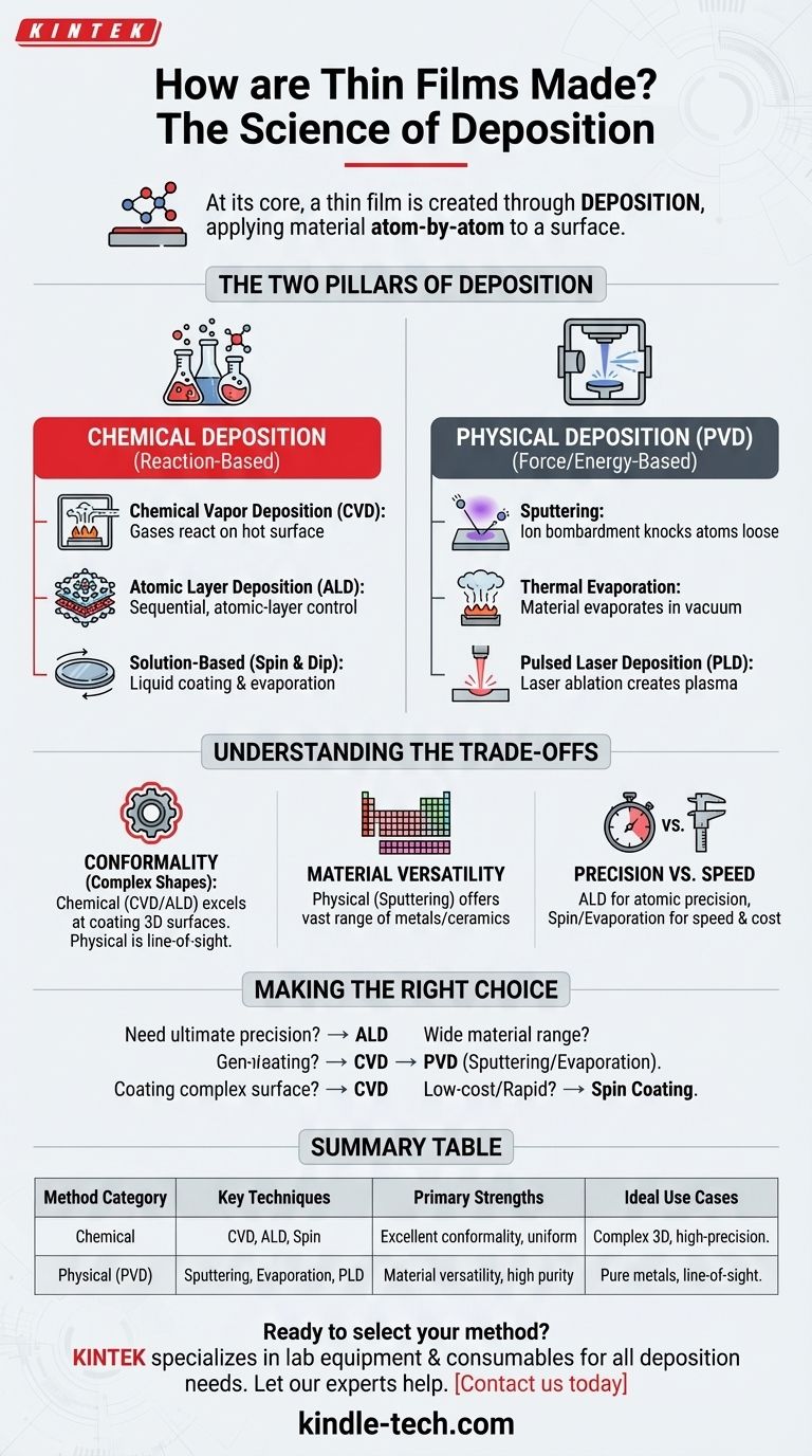
At its core, a thin film is created through a process called deposition, where material is carefully applied to a surface, known as a substrate. These methods are broadly divided into two fundamental categories: those that use chemical reactions to form the film, and those that use physical force or energy to transfer the material. This precision allows for the creation of layers that can be as thin as a single atom.
The essential difference in making thin films lies not in the specific machine used, but in the core strategy: either building the film through controlled chemical reactions on a surface or by physically transferring material atom-by-atom in a vacuum. The choice between these two paths dictates the film's cost, purity, and ultimate performance.
The Two Pillars of Thin Film Deposition
All techniques for creating thin films fall under two primary umbrellas: Chemical Deposition and Physical Deposition. Understanding this distinction is the first step in understanding the entire field.
Understanding Chemical Deposition
Chemical deposition methods use a chemical reaction to synthesize the film directly on the substrate from precursor materials. These precursors are often liquids or gases that react and leave behind a solid layer.
Chemical Vapor Deposition (CVD)
In CVD, the substrate is placed in a chamber and exposed to volatile precursor gases. These gases react or decompose on the substrate's hot surface, forming the desired thin film.
Atomic Layer Deposition (ALD)
ALD is a more precise subtype of CVD. It relies on sequential, self-limiting chemical reactions, allowing for the deposition of material literally one atomic layer at a time, providing exceptional control over thickness and uniformity.
Solution-Based Methods (Spin & Dip Coating)
These simpler methods involve coating the substrate with a liquid chemical solution. In spin coating, the substrate is spun at high speed to spread the liquid into a thin, uniform layer. The solvent then evaporates, leaving the solid film behind.
Understanding Physical Deposition
Physical Vapor Deposition (PVD) methods do not involve chemical reactions. Instead, they use mechanical, thermal, or electrical means to transport material from a source "target" and deposit it onto the substrate, typically within a high-vacuum environment.
Sputtering
In sputtering, a target made of the desired film material is bombarded with high-energy ions (a plasma). This bombardment physically knocks atoms loose from the target, which then travel and deposit onto the substrate, forming the film.
Thermal Evaporation
This method involves heating the source material in a vacuum chamber until it evaporates. The vaporized atoms then travel in a straight line until they condense on the cooler substrate, much like steam condensing on a cold mirror.
Pulsed Laser Deposition (PLD)
In PLD, a high-power laser is aimed at the target material. The intense energy ablates (vaporizes) a small amount of the material into a plasma plume, which then deposits onto the substrate.
Understanding the Trade-offs
No single deposition method is universally superior. The choice is always a matter of balancing project requirements like cost, material compatibility, required precision, and the shape of the object being coated.
Conformality: Coating Complex Shapes
Chemical methods, particularly CVD and ALD, excel at creating highly conformal coatings. Because the precursor gases can reach every nook and cranny, they can uniformly coat complex, three-dimensional surfaces. PVD methods are "line-of-sight" and struggle to coat shadowed areas.
Material Versatility
Physical methods, especially sputtering, are extremely versatile. They can be used to deposit a vast range of materials, including pure metals, alloys, and ceramics, that are difficult or impossible to create with chemical precursors.
Precision vs. Production Speed
Techniques offering the highest precision, like ALD or Molecular Beam Epitaxy (MBE), are often slower and more expensive processes. In contrast, methods like spin coating or thermal evaporation can be much faster and more cost-effective for larger areas or high-volume production where atomic-level perfection isn't necessary.
Making the Right Choice for Your Goal
Selecting a method requires clearly defining your primary objective.
- If your primary focus is ultimate precision and uniformity: ALD is the superior choice for its atomic-level control.
- If your primary focus is coating a complex, non-flat surface: A chemical method like CVD will provide the best coverage.
- If your primary focus is depositing a wide range of pure metals or inorganic compounds: PVD methods like sputtering or evaporation offer the most flexibility.
- If your primary focus is low-cost production or rapid prototyping: Simpler, solution-based methods like spin coating are often the most practical starting point.
Ultimately, selecting the correct deposition technique is about matching the physical or chemical process to the specific material properties your application demands.
Summary Table:
| Method Category | Key Techniques | Primary Strengths | Ideal Use Cases |
|---|---|---|---|
| Chemical Deposition | CVD, ALD, Spin Coating | Excellent conformality, uniform coatings | Complex 3D surfaces, high-precision layers |
| Physical Deposition (PVD) | Sputtering, Thermal Evaporation, PLD | Material versatility, high purity | Pure metals, alloys, line-of-sight coatings |
Ready to select the perfect thin film deposition method for your application? KINTEK specializes in lab equipment and consumables for all your deposition needs. Whether you require the precision of ALD, the versatility of sputtering, or the cost-effectiveness of spin coating, our experts can help you choose the right solution. Contact us today to discuss your project and discover how KINTEK can enhance your laboratory's capabilities!
Visual Guide
Related Products
- Chemical Vapor Deposition CVD Equipment System Chamber Slide PECVD Tube Furnace with Liquid Gasifier PECVD Machine
- Microwave Plasma Chemical Vapor Deposition MPCVD Machine System Reactor for Lab and Diamond Growth
- 915MHz MPCVD Diamond Machine Microwave Plasma Chemical Vapor Deposition System Reactor
- Customer Made Versatile CVD Tube Furnace Chemical Vapor Deposition Chamber System Equipment
- HFCVD Machine System Equipment for Drawing Die Nano-Diamond Coating
People Also Ask
- How are carbon nanotubes grown? Master Scalable Production with Chemical Vapor Deposition
- Why is Chemical Vapor Deposition (CVD) equipment uniquely suited for constructing hierarchical superhydrophobic structures?
- What happens during deposition chemistry? Building Thin Films from Gaseous Precursors
- What are the core advantages of PE-CVD in OLED encapsulation? Protect Sensitive Layers with Low-Temp Film Deposition
- How expensive is chemical vapor deposition? Understanding the True Cost of High-Performance Coating


