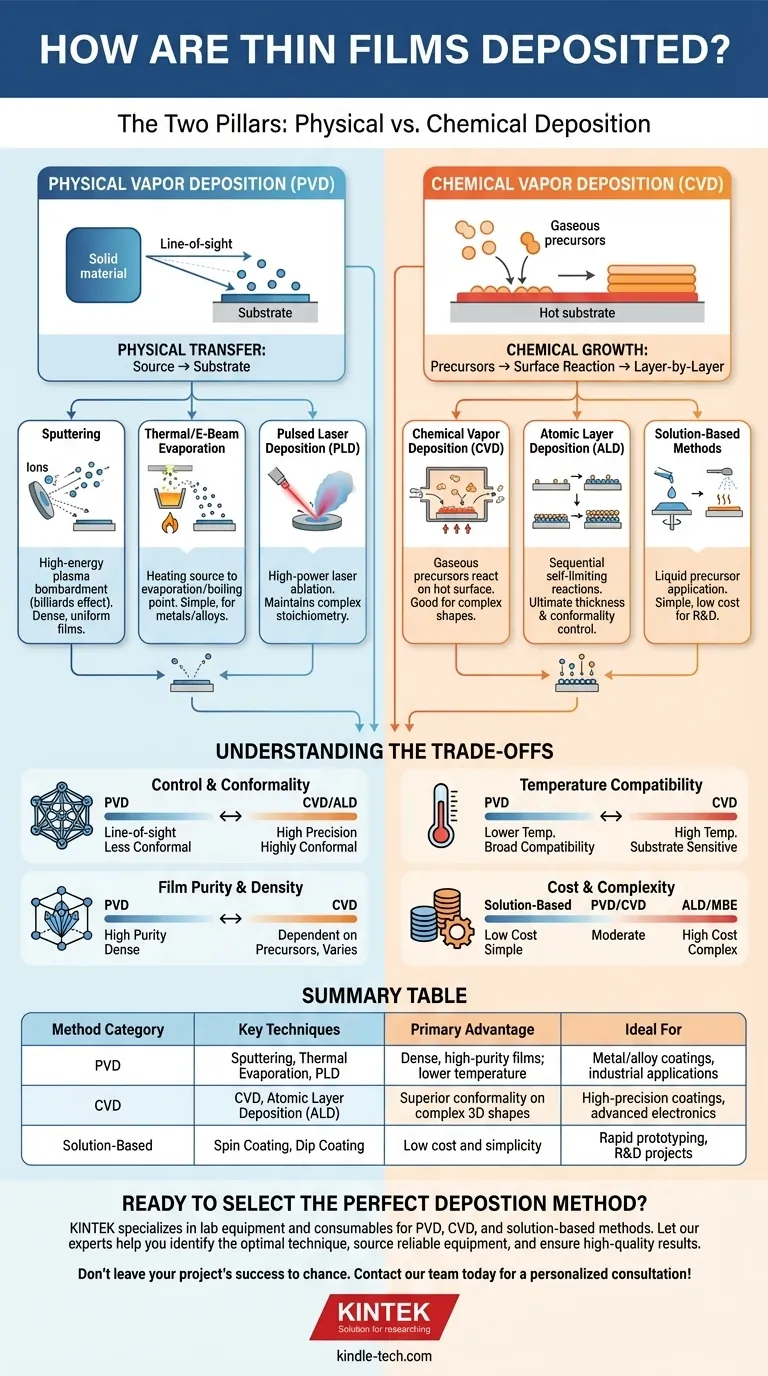
At its core, thin film deposition is accomplished through two primary families of techniques: Physical Vapor Deposition (PVD) and Chemical Vapor Deposition (CVD). PVD involves physically transferring a material from a source to a substrate—think of it as spray-painting with individual atoms. In contrast, CVD uses chemical reactions between precursor gases on the substrate’s surface to grow the film layer by layer.
The fundamental choice is not just about the method, but about the underlying mechanism. Selecting between a physical transfer process (PVD) and a chemical growth process (CVD) is the most critical decision, as it dictates the film's properties, uniformity, and cost.
The Two Pillars: Physical vs. Chemical Deposition
All thin film deposition techniques fall into one of two major categories. Understanding the difference between them is the key to understanding the entire field.
Physical Vapor Deposition (PVD): Transferring the Material
PVD methods move solid material from a source (the "target") to the substrate without changing its chemical composition. These are often "line-of-sight" processes, meaning the atoms travel in a straight line from the source to the surface they coat.
Sputtering
Sputtering is a highly versatile PVD workhorse. It uses a high-energy plasma (typically from a gas like Argon) to bombard a target material.
This bombardment acts like a microscopic game of billiards, knocking atoms loose from the target. These ejected atoms then travel through a vacuum and deposit onto the substrate, forming a dense and uniform film.
Thermal Evaporation
This is one of the conceptually simplest methods. The source material is heated in a high vacuum chamber until it begins to evaporate, or "boil."
These evaporated atoms travel through the vacuum and condense on the cooler substrate, much like steam condensing on a cold mirror. A more advanced version, Electron Beam Evaporation, uses a focused beam of electrons to heat materials with very high melting points.
Pulsed Laser Deposition (PLD)
In PLD, a high-power laser beam is focused onto the target material inside the vacuum chamber. The intense energy instantly vaporizes, or "ablates," a small amount of the material, creating a plume of plasma.
This plasma plume expands from the target and deposits as a thin film onto the substrate. This method is excellent for maintaining the complex stoichiometry of multi-element materials.
Chemical Methods: Growing the Film
Chemical deposition methods use chemical reactions to create the film. This often allows for better coverage on complex, non-flat surfaces.
Chemical Vapor Deposition (CVD)
In a typical CVD process, the substrate is placed in a reaction chamber and heated. Precursor gases containing the required elements are then introduced.
These gases react on the hot surface of the substrate, forming the desired solid film and volatile byproducts, which are then pumped away.
Atomic Layer Deposition (ALD)
ALD is an advanced form of CVD that offers the ultimate control over film thickness and conformality. It builds the film one single atomic layer at a time.
The process uses a sequence of self-limiting chemical reactions. Each step adds exactly one monolayer of a material, allowing for unparalleled precision and the ability to perfectly coat extremely complex 3D structures.
Solution-Based Methods (Sol-Gel, Spin Coating)
These are liquid-phase chemical techniques often valued for their simplicity and low cost. They involve applying a liquid precursor—a sol or gel—onto the substrate.
Techniques like spin coating (spinning the substrate to spread the liquid), dip coating (dipping it in the solution), or spray pyrolysis are used for application. The film is then formed by drying and thermally treating the substrate to solidify the precursor into its final form.
Understanding the Trade-offs
Choosing a deposition method is a matter of engineering trade-offs. No single technique is best for every application.
Control and Conformality
CVD processes, and especially ALD, excel at creating highly conformal films. This means they can uniformly coat intricate, high-aspect-ratio trenches and 3D shapes. PVD methods are largely line-of-sight and struggle to coat "shadowed" areas.
Temperature and Substrate Compatibility
Many CVD processes require very high temperatures to drive the chemical reactions. This can damage sensitive substrates like polymers or certain electronic components. PVD methods like sputtering can often be performed at much lower temperatures, making them more broadly compatible.
Film Purity and Density
PVD methods, particularly sputtering, are known for producing very dense films with high purity. CVD film quality is highly dependent on the purity of the precursor gases and the precise control of reaction conditions.
Cost and Complexity
Solution-based methods are typically the cheapest and simplest, making them ideal for research and development. Sputtering and thermal evaporation represent a moderate cost for high-quality industrial production. ALD and Molecular Beam Epitaxy (MBE), an ultra-high vacuum PVD technique, are at the highest end of cost and complexity, reserved for cutting-edge applications.
Making the Right Choice for Your Goal
Your application's primary driver will determine the best deposition strategy.
- If your primary focus is ultimate precision and uniform coating on complex shapes: Atomic Layer Deposition (ALD) is the superior choice for its angstrom-level, layer-by-layer control.
- If your primary focus is depositing dense, high-quality metal or alloy films for industrial use: Sputtering offers a robust and versatile balance of performance and cost.
- If your primary focus is rapid prototyping or low-cost lab-scale experiments: Solution-based methods like spin coating or dip coating provide the simplest and most accessible starting point.
- If your primary focus is growing ultra-high-purity crystalline films for advanced electronics or research: Molecular Beam Epitaxy (MBE) or a specialized CVD process are the industry standards.
Understanding these core principles allows you to move beyond simply knowing the methods to strategically selecting the right tool for your specific engineering challenge.
Summary Table:
| Method Category | Key Techniques | Primary Advantage | Ideal For |
|---|---|---|---|
| Physical Vapor Deposition (PVD) | Sputtering, Thermal Evaporation, PLD | Dense, high-purity films; lower temperature | Metal/alloy coatings, industrial applications |
| Chemical Vapor Deposition (CVD) | CVD, Atomic Layer Deposition (ALD) | Superior conformality on complex 3D shapes | High-precision coatings, advanced electronics |
| Solution-Based Methods | Spin Coating, Dip Coating | Low cost and simplicity | Rapid prototyping, R&D projects |
Ready to Select the Perfect Deposition Method for Your Project?
Choosing the right thin film deposition technique is critical to achieving the film properties, uniformity, and cost-efficiency your project demands. KINTEK specializes in providing the lab equipment and consumables you need to succeed, whether you're working with PVD, CVD, or solution-based methods.
Let our experts help you:
- Identify the optimal technique for your specific material and substrate.
- Source reliable equipment for sputtering, evaporation, ALD, and more.
- Ensure your lab is equipped for high-quality, reproducible results.
Don't leave your project's success to chance. Contact our team today for a personalized consultation!
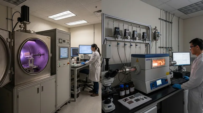
Visual Guide
Related Products
- Aluminized Ceramic Evaporation Boat for Thin Film Deposition
- Tungsten Evaporation Boat for Thin Film Deposition
- Electron Beam Evaporation Coating Oxygen-Free Copper Crucible and Evaporation Boat
- Molybdenum Tungsten Tantalum Evaporation Boat for High Temperature Applications
- Vacuum Hot Press Furnace Machine for Lamination and Heating
People Also Ask
- What is the chemical method for thin film deposition? Build Films from the Molecular Level Up
- What is the source of evaporation for thin film? Choosing Between Thermal and E-Beam Methods
- Why is an alumina boat and Ti3AlC2 powder bed necessary for Ti2AlC sintering? Protect MAX Phase Purity
- What are the applications of thin films deposition? Unlock New Possibilities for Your Materials
- What is the widely used boat made of in thermal evaporation? Choosing the Right Material for High-Purity Deposition


