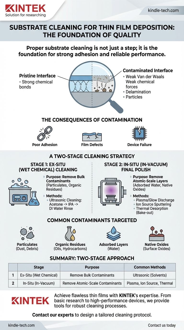
Proper substrate cleaning is not a preliminary step; it is the foundation of high-quality thin film deposition. The process typically involves a multi-stage approach, beginning with ex-situ chemical cleaning using solvents in an ultrasonic bath to remove bulk contaminants. This is followed by a critical in-situ cleaning stage inside the vacuum chamber using methods like plasma treatment or ion sources to remove the final atomic layers of contamination just before deposition begins.
Substrate cleaning is a systematic process designed to eliminate contaminants at every scale, from visible dust and oils to invisible monolayers of adsorbed water and native oxides. Failing to achieve a truly pristine surface is the most common cause of poor film adhesion, inconsistent properties, and device failure.
The Critical Role of a Pristine Surface
To create a high-integrity thin film, the deposited atoms must form a strong, direct bond with the substrate atoms. Any intervening contaminant layer acts as a weak point, compromising the entire structure.
Why Cleaning Dictates Film Success
A contaminated surface fundamentally prevents proper film adhesion. Atoms from the deposition process land on a layer of oil, water, or dust instead of the substrate itself, leading to weak Van der Waals forces instead of strong chemical bonds.
This poor adhesion is the primary cause of film stress, peeling, and delamination, which results in the complete failure of the device or coating.
The Impact on Film Properties
Contaminants are essentially defects. They disrupt the uniform growth of the film, creating inconsistencies in its structure and density.
These structural flaws directly degrade the film's functional properties. For optical coatings, this can mean reduced transparency or incorrect reflectivity. For electronic films, it can lead to higher electrical resistance, shorts, or unpredictable performance.
The Enemies: Common Contaminants
Cleaning strategies are designed to target four main categories of contaminants:
- Particulates: Dust, fibers, and other loose debris.
- Organic Residues: Oils from handling (fingerprints), machining fluids, and atmospheric hydrocarbons.
- Adsorbed Layers: Primarily water molecules from ambient humidity that quickly form a thin layer on any exposed surface.
- Native Oxides: A thin layer of oxide that naturally forms on many materials (like silicon or aluminum) when exposed to air.
A Two-Stage Cleaning Strategy
An effective cleaning protocol is a one-two punch: a gross cleaning outside the chamber followed by an atomic-level polish inside the chamber.
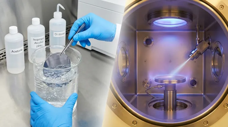
Stage 1: Ex-Situ (Wet Chemical) Cleaning
This is the first line of defense, designed to remove bulk organic and particulate contamination. The most common method is ultrasonic cleaning.
The substrate is submerged in a sequence of solvents—typically acetone, then isopropyl alcohol (IPA), and finally deionized (DI) water. The high-frequency sound waves create microscopic cavitation bubbles that scrub the surface clean.
Stage 2: In-Situ (In-Vacuum) Final Polish
After the substrate is loaded into the deposition chamber and vacuum is achieved, a final cleaning is performed to remove the microscopic layers that remain.
Plasma or Glow Discharge Cleaning is a common technique. A low-pressure gas (like Argon or Oxygen) is energized with an RF field, creating a plasma. The energetic ions gently bombard the surface, sputtering away the final contaminants.
Ion Source Cleaning offers a more controlled approach. A dedicated ion gun generates a focused beam of ions that can be directed at the substrate to physically sputter away contaminants and even stubborn native oxides.
Thermal Desorption (Preheating) involves heating the substrate in a vacuum. This "bakes off" adsorbed water molecules and other volatile contaminants, which are then removed by the vacuum pump. This is often used in conjunction with other in-situ methods.
Understanding the Trade-offs
No single method is perfect for every situation. Understanding their limitations is key to designing a robust process.
Wet Chemical Cleaning Limitations
While essential for removing gross contamination, solvent cleaning is never the final step. The process itself can leave behind trace residues, and the substrate is immediately re-contaminated by atmospheric water vapor the moment it is removed from the DI water.
Plasma and Ion Source Considerations
These methods are extremely effective but can be too aggressive if not controlled. High-energy ion bombardment can introduce damage to the substrate's crystal structure or implant ions, altering the surface's properties. The choice of gas is also critical: Argon is inert and used for physical sputtering, while Oxygen is reactive and excellent for "ashing" (chemically burning off) organic residues.
The Consequence of Insufficient Cleaning
Skipping or poorly executing the cleaning protocol directly leads to low-yield production. The resulting films will suffer from poor adhesion, delamination, and inconsistent electrical or optical properties, ultimately raising costs and reducing reliability.
Making the Right Choice for Your Application
Your cleaning strategy must match the sensitivity of your final film.
- If your primary focus is basic material research or non-critical coatings: A thorough ultrasonic solvent clean followed by in-situ thermal preheating to remove water may be sufficient.
- If your primary focus is high-performance optical or electronic devices: A multi-stage process is non-negotiable, requiring ultrasonic cleaning followed by an in-situ plasma or ion source treatment.
- If your primary focus is removing a stubborn native oxide (e.g., on a silicon wafer): An in-situ Argon ion source or RF plasma treatment is the standard method to sputter the oxide away immediately before deposition.
- If your primary focus is ensuring removal of all organic residues: An Oxygen plasma is highly effective for chemically ashing any remaining hydrocarbon contamination.
Ultimately, treating the substrate surface with the same precision as the deposition process itself is the key to achieving reliable, high-performance thin films.
Summary Table:
| Cleaning Stage | Purpose | Common Methods |
|---|---|---|
| Ex-Situ (Wet Chemical) | Remove bulk contaminants (oils, particulates) | Ultrasonic cleaning with solvents (acetone, IPA, DI water) |
| In-Situ (In-Vacuum) | Remove atomic-scale contaminants (water, oxides) | Plasma treatment, ion source sputtering, thermal desorption |
Achieve flawless thin films with KINTEK's expertise in substrate preparation.
Your thin film's performance starts with the substrate. Contamination is the leading cause of film failure, leading to costly rework and low yields. KINTEK specializes in lab equipment and consumables for laboratory needs, providing the tools and knowledge for a robust, reliable cleaning process tailored to your application—from basic research to high-performance electronic devices.
Contact our experts today to discuss your specific substrate and deposition requirements. We'll help you design a cleaning protocol that ensures strong adhesion, consistent film properties, and maximum device reliability.
Visual Guide
Related Products
People Also Ask
- Why are PTFE containers required for PCT leaching tests? Ensure Chemical Inertness and Analytical Precision
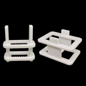
- What is the maximum operating temperature for a PTFE cleaning basket? Avoid Catastrophic Failure at 260°C
- What material is a PTFE cleaning basket made of? Unlocking Superior Chemical and Thermal Resistance
- What should be monitored during the cleaning process when using a PTFE cleaning basket? Ensure Reliable Results & Prevent Damage
- What is the procedure for using a PTFE cleaning basket? A 3-Step Guide for Flawless Results