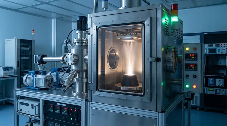
At its core, an electron beam evaporator is a sophisticated tool that uses a high-energy beam of electrons to heat and vaporize a source material inside a high-vacuum chamber. This process, a form of Physical Vapor Deposition (PVD), generates a vapor stream that condenses onto a target substrate, forming an exceptionally pure and uniform thin film.
Electron beam evaporation offers unparalleled purity and control for depositing thin films, especially for high-melting-point materials. Its key is the direct conversion of an electron's kinetic energy into thermal energy, but this precision comes with the inherent complexities of high-voltage and high-vacuum systems.
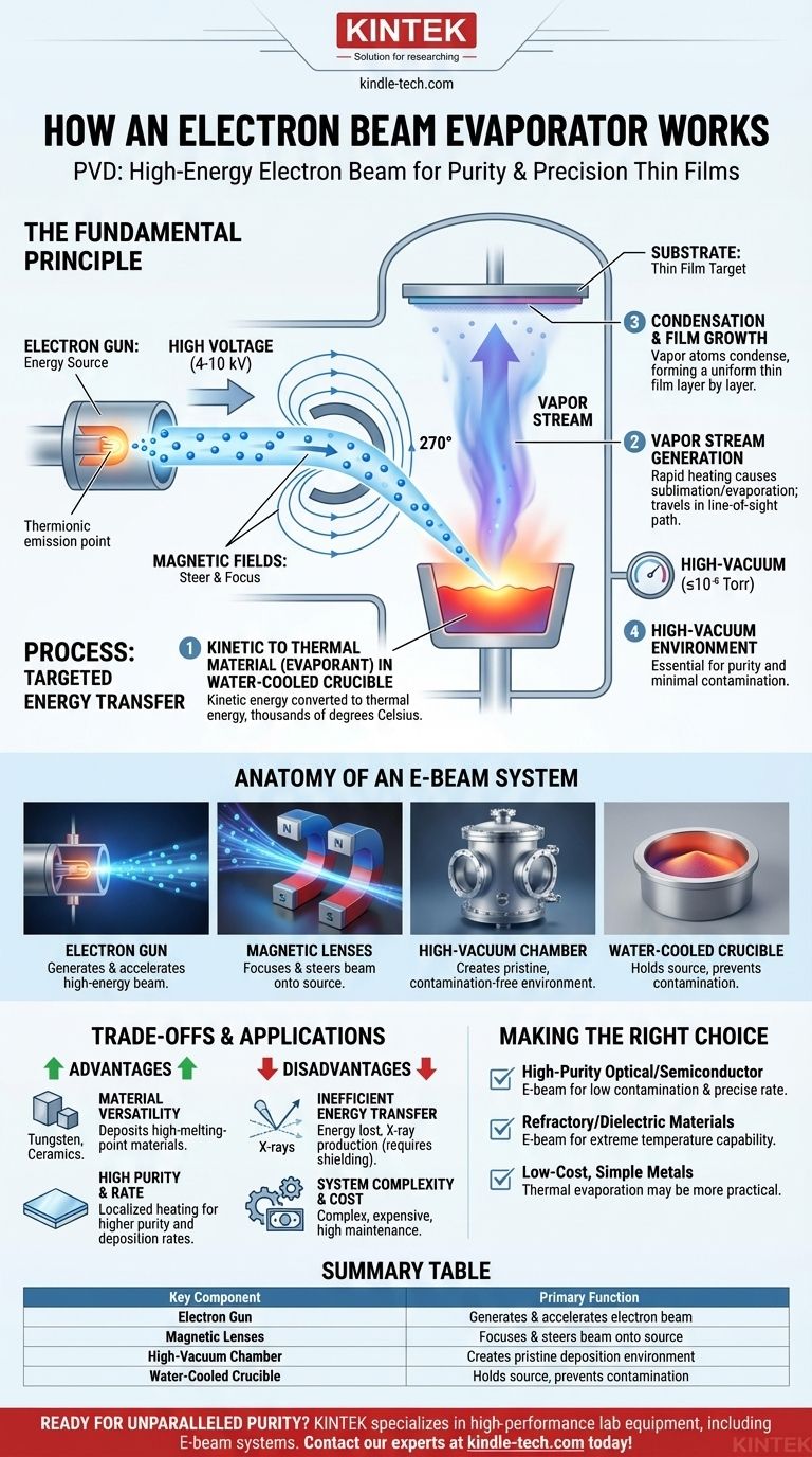
The Fundamental Principle: Targeted Energy Transfer
Converting Kinetic Energy to Heat
The entire process hinges on a simple physics principle. A focused beam of high-energy electrons, accelerated by a high voltage, is directed to strike a source material (the evaporant) held in a crucible.
When the electrons collide with the material, their kinetic energy is instantaneously converted into thermal energy. This intense, localized heating raises the surface temperature of the material directly, often to several thousand degrees Celsius.
Generating a Vapor Stream
This rapid temperature increase is sufficient to cause the material to sublimate or evaporate, releasing a plume of vapor. Because this occurs in a high-vacuum environment, the vapor travels in a straight, line-of-sight path with minimal contamination from atmospheric gases.
Condensation and Film Growth
A substrate (the object to be coated) is strategically placed within this vapor stream. As the vapor atoms or molecules strike the cooler substrate surface, they condense and adhere, gradually building up a thin, solid film layer by layer.
The Anatomy of an E-Beam System
The Electron Gun: The Energy Source
The process begins with the electron gun, which generates the beam. A tungsten filament is heated to a point of thermionic emission, causing it to release a cloud of electrons.
These free electrons are then accelerated toward an anode by a powerful electric field, typically created by a voltage of 4 to 10 kilovolts (kV). This acceleration is what gives the electrons their high kinetic energy.
Magnetic Fields: Steering and Focusing
Unlike light, electron beams can be precisely steered and focused using magnetic fields. Electromagnets located outside the crucible are used to bend the electron beam, often by 270 degrees.
This bending serves two critical purposes. First, it allows the fragile filament of the electron gun to be positioned below the crucible, shielding it from falling evaporant material. Second, it allows for precise control over where the beam strikes the source material, enabling uniform heating and evaporation.
The Vacuum Chamber: A Pristine Environment
The entire process takes place within a high-vacuum chamber, typically pumped down to pressures of 10⁻⁶ Torr or lower.
This vacuum is essential for preventing the electron beam from scattering off air molecules and, more importantly, for ensuring the purity of the final film by removing contaminants that could otherwise react with the vapor stream.
Understanding the Trade-offs and Limitations
Advantage: Material Versatility
Because the heating is so intense and direct, e-beam evaporation can be used to deposit materials with extremely high melting points, such as tungsten, tantalum, and various ceramics, which are difficult or impossible to evaporate using other methods.
Advantage: High Purity and Deposition Rate
Heating is localized only to the surface of the source material. This prevents the entire crucible from melting and introducing contaminants into the vapor stream, resulting in higher-purity films compared to thermal evaporation. The high energy density also allows for very high deposition rates.
Disadvantage: Inefficient Energy Transfer and X-Rays
The energy conversion is not perfectly efficient. Some energy is lost to back-scattered electrons, secondary electrons, and, most significantly, the generation of X-rays.
This X-ray production is an unavoidable byproduct of high-energy electrons striking a target. It requires proper shielding to ensure operator safety and can sometimes damage sensitive substrates.
Disadvantage: System Complexity and Cost
E-beam evaporators are significantly more complex and expensive than simpler thermal evaporation systems. They require high-voltage power supplies, sophisticated magnetic field controls, and robust high-vacuum systems, all of which contribute to higher operational and maintenance costs.
Making the Right Choice for Your Application
Choosing a deposition method depends entirely on your technical requirements and constraints.
- If your primary focus is depositing high-purity optical coatings or semiconductor layers: E-beam evaporation is an excellent choice due to its low contamination and precise rate control.
- If your primary focus is coating with refractory metals or dielectric materials: E-beam's ability to reach extremely high temperatures makes it one of the few viable options.
- If your primary focus is low-cost, simple metal coatings on robust substrates: A less complex method like thermal evaporation might be a more practical and cost-effective solution.
Ultimately, understanding this balance of power, precision, and complexity is the key to leveraging electron beam evaporation effectively in your work.
Summary Table:
| Key Component | Primary Function |
|---|---|
| Electron Gun | Generates and accelerates a high-energy beam of electrons. |
| Magnetic Lenses | Focuses and steers the electron beam onto the source material. |
| High-Vacuum Chamber | Creates a pristine environment for contamination-free deposition. |
| Water-Cooled Crucible | Holds the source material while preventing contamination from melt. |
Ready to achieve unparalleled thin film purity and performance?
Electron beam evaporation is ideal for demanding applications in optics, semiconductors, and research. KINTEK specializes in high-performance lab equipment, including e-beam evaporation systems, to meet your precise deposition needs.
Contact our experts today to discuss how our solutions can enhance your laboratory's capabilities. Get in touch via our contact form to start the conversation.
Visual Guide
Related Products
- Electron Beam Evaporation Coating Tungsten Crucible and Molybdenum Crucible for High Temperature Applications
- Electron Beam Evaporation Coating Oxygen-Free Copper Crucible and Evaporation Boat
- Electron Beam Evaporation Coating Gold Plating Tungsten Molybdenum Crucible for Evaporation
- Electron Beam Evaporation Coating Conductive Boron Nitride Crucible BN Crucible
- High Purity Pure Graphite Crucible for Electron Beam Evaporation
People Also Ask
- What is the deposition rate of e-beam evaporation? Control Thin Film Quality and Speed
- What is the process of e-beam coating? Achieve High-Purity, Precise Thin Films for Your Lab
- What materials are used in electron beam evaporation? Master High-Purity Thin Film Deposition
- What is e-beam evaporation? Achieve High-Purity Thin Film Deposition for Your Lab
- What is e-beam evaporation used for? Precision Coating for Optics, Aerospace & Electronics


