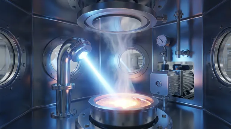
Electron beam evaporation is a physical vapor deposition (PVD) process that uses a focused stream of high-energy electrons to vaporize a source material inside a high-vacuum chamber. This intense, localized heating turns the material into a vapor, which then travels and condenses onto a substrate, forming an exceptionally pure and dense thin film.
The core challenge in thin-film manufacturing is depositing a pure material without contaminating it or damaging the substrate. Electron beam evaporation solves this by using a precisely controlled beam of electrons as a "scalpel" of heat, targeting only the source material and ensuring an ultra-clean deposition environment.
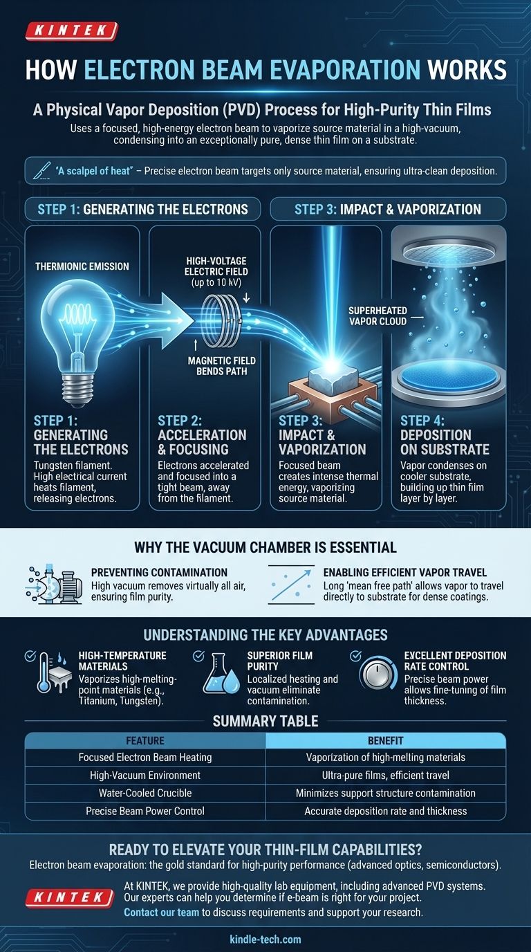
The Core Mechanism: From Electron to Film
To understand how the process works, it's best to break it down into four distinct, sequential steps. Each stage is critical for achieving a high-quality final coating.
Step 1: Generating the Electrons
The process begins with a tungsten filament, known as the cathode. A high electrical current is passed through this filament, causing it to heat up significantly.
This intense heat gives the electrons in the tungsten enough energy to escape from its surface, a phenomenon known as thermionic emission.
Step 2: Acceleration and Focusing
Once freed, the cloud of electrons is accelerated toward the source material by a powerful high-voltage electric field, often up to 10 kV.
A carefully configured magnetic field then bends the path of these high-speed electrons, focusing them into a tight, precise beam. This prevents the hot filament from being in the direct line-of-sight of the evaporating material, extending its life and reducing contamination.
Step 3: Impact and Vaporization
The focused electron beam strikes the surface of the source material, which is held in a water-cooled copper hearth or crucible.
Upon impact, the immense kinetic energy of the electrons is instantly converted into thermal energy. This creates a small, superheated spot on the material, causing it to either melt and then evaporate or sublimate directly from a solid to a gas.
Step 4: Deposition on the Substrate
The resulting vapor cloud expands from the source and travels through the vacuum chamber.
When the vapor atoms or molecules reach the cooler surface of the substrate, they condense back into a solid state, gradually building up the desired thin film layer by layer.
Why the Vacuum Chamber is Essential
The entire process takes place under high vacuum for two critical reasons that directly impact the quality of the final film.
Preventing Contamination
A high vacuum removes virtually all air molecules, such as oxygen and nitrogen, from the chamber. This ensures the vaporized material doesn't react with unwanted gases on its way to the substrate, resulting in a film of exceptionally high purity.
Enabling Efficient Vapor Travel
In a vacuum, there are very few molecules for the vapor atoms to collide with. This creates a long "mean free path," allowing the material to travel in a straight line from the source to the substrate, which is essential for creating dense and uniform coatings.
Understanding the Key Advantages
Electron beam evaporation is chosen over other deposition methods for its unique capabilities and the high quality of the films it produces.
Advantage: High-Temperature Materials
The focused energy of the electron beam is so intense that it can vaporize materials with extremely high melting points, such as refractory metals and ceramics. These materials are often impossible to deposit using simpler thermal evaporation techniques.
Advantage: Superior Film Purity
Because the electron beam heats only the source material and not the crucible itself (which is actively water-cooled), contamination from the support structure is virtually eliminated. This, combined with the high vacuum, leads to some of the purest films possible.
Advantage: Excellent Deposition Rate Control
The power of the electron beam can be precisely controlled, allowing for fine-tuning of the material's evaporation rate. This gives operators exceptional control over the thickness and growth of the thin film.
Making the Right Choice for Your Application
Choosing a deposition method depends entirely on your material requirements and performance goals.
- If your primary focus is depositing high-melting-point materials like titanium or tungsten: Electron beam evaporation is one of the most effective and reliable methods available.
- If your primary focus is achieving the highest possible film purity for optical or electronic applications: The clean, localized heating and high-vacuum environment make this the superior choice.
- If you need precise control over film thickness and deposition speed: The fine control over beam power gives you the ability to manage film growth with high accuracy.
Ultimately, electron beam evaporation is a powerful manufacturing process for creating high-performance coatings that are simply not achievable with other methods.
Summary Table:
| Feature | Benefit |
|---|---|
| Focused Electron Beam Heating | Enables vaporization of high-melting-point materials like tungsten and ceramics. |
| High-Vacuum Environment | Ensures ultra-pure films by preventing contamination and enabling efficient vapor travel. |
| Water-Cooled Crucible | Minimizes contamination from the source material's support structure. |
| Precise Beam Power Control | Allows for accurate control over deposition rate and final film thickness. |
Ready to elevate your thin-film deposition capabilities?
Electron beam evaporation is the gold standard for applications demanding the highest levels of purity and performance, from advanced optics to semiconductor components.
At KINTEK, we specialize in providing high-quality lab equipment, including advanced PVD systems, to meet the precise needs of your laboratory. Our experts can help you determine if e-beam evaporation is the right solution for your project and provide the reliable equipment you need to succeed.
Contact our team today to discuss your specific requirements and discover how KINTEK can support your research and development goals.
Visual Guide
Related Products
- Electron Beam Evaporation Coating Tungsten Crucible and Molybdenum Crucible for High Temperature Applications
- Electron Beam Evaporation Coating Oxygen-Free Copper Crucible and Evaporation Boat
- Electron Beam Evaporation Coating Gold Plating Tungsten Molybdenum Crucible for Evaporation
- Electron Beam Evaporation Coating Conductive Boron Nitride Crucible BN Crucible
- E Beam Crucibles Electron Gun Beam Crucible for Evaporation
People Also Ask
- What is the process of e-beam coating? Achieve High-Purity, Precise Thin Films for Your Lab
- What is the voltage of e-beam evaporation? Achieve Precise Thin-Film Deposition
- What is the current of e-beam evaporation? A Guide to High-Purity Thin Film Deposition
- What is the container that holds the metal source material called in e-beam evaporation? Ensure Purity and Quality in Your Thin-Film Deposition
- What is the temperature of e-beam evaporation? Mastering the Two-Zone Thermal Process for Precision Films


