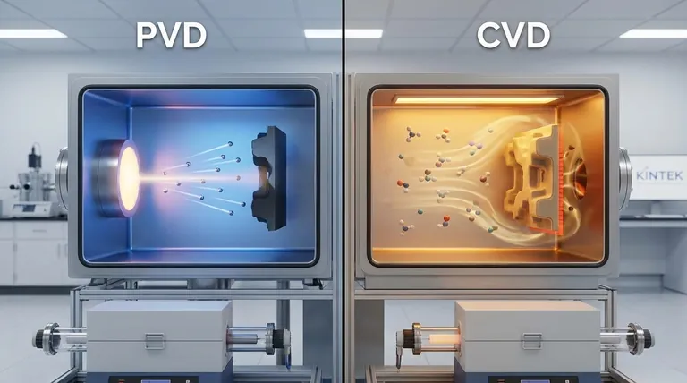
At their core, the fundamental difference is that Physical Vapor Deposition (PVD) is a physical process, while Chemical Vapor Deposition (CVD) is a chemical one. PVD works by vaporizing a solid material in a vacuum and having it condense atom-by-atom onto a substrate. In contrast, CVD exposes a substrate to volatile precursor gases which react or decompose on the surface to form the desired solid film.
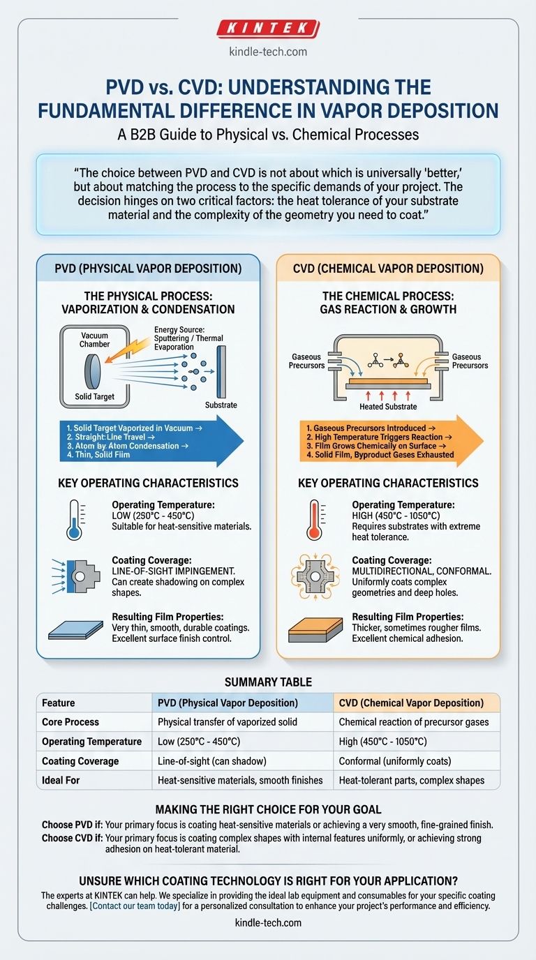
The choice between PVD and CVD is not about which is universally "better," but about matching the process to the specific demands of your project. The decision hinges on two critical factors: the heat tolerance of your substrate material and the complexity of the geometry you need to coat.
The Fundamental Process: Physical vs. Chemical
The names "Physical" and "Chemical" vapor deposition are not arbitrary; they describe the essence of how each process works. This core difference dictates their operating parameters and ideal applications.
How PVD Works: A Physical Transfer
In PVD, the coating material starts as a solid target. This target is bombarded with energy (e.g., via sputtering or thermal evaporation) inside a vacuum chamber, causing atoms or molecules to break free and travel through the vacuum.
These vaporized particles travel in a straight line until they strike the substrate, where they cool and condense to form a thin, solid film. This is a line-of-sight process, much like spray painting.
How CVD Works: A Chemical Reaction
CVD begins with gaseous precursor molecules. These gases are introduced into a reaction chamber containing the heated substrate.
The high temperature provides the energy needed to trigger a chemical reaction on the substrate's surface. This reaction "grows" a solid film directly onto the part, with byproduct gases being exhausted. The coating is formed by a chemical transformation, not a simple physical transfer.
Key Distinctions in Practice
The difference between a physical transfer and a chemical reaction creates several practical distinctions that directly impact which method you should choose.
Operating Temperature
This is often the most critical deciding factor. PVD operates at significantly lower temperatures (typically 250°C to 450°C), making it suitable for a wider range of materials, including some heat-treated steels and alloys that would be compromised by higher heat.
CVD requires much higher temperatures (often 450°C to 1050°C) to drive the necessary chemical reactions. This limits its use to substrates that can withstand extreme heat without deforming or losing their material properties.
Coating Geometry and Coverage
PVD is a line-of-sight impingement process. Any surface not in the direct path of the vaporized material will not be coated, creating a "shadowing" effect on complex parts.
CVD is a multidirectional, conformal process. Because the deposition is driven by a gas that surrounds the entire part, it can uniformly coat complex shapes, deep holes, and internal surfaces with ease.
Resulting Film Properties
The processes yield different types of films. PVD typically produces very thin, smooth, and durable coatings. It offers excellent control over the final surface finish.
CVD can create thicker and sometimes rougher films. However, the chemical bonding often results in excellent adhesion to the substrate.
Understanding the Trade-offs
Neither method is a perfect solution for all scenarios. Understanding their inherent limitations is key to making an informed decision.
Cost and Complexity
While costs vary by application, PVD can be more expensive for some projects due to the need for complex fixtures to rotate parts and mitigate the line-of-sight issue.
CVD is often more economical for batch processing of many parts at once, especially if those parts have complex geometries that PVD cannot handle efficiently.
Material and Substrate Limitations
The primary limitation of CVD is its high operating temperature, which immediately disqualifies many common engineering materials.
PVD's main limitation is its inability to uniformly coat intricate shapes without complex and potentially costly mechanical rotation of the parts during the process.
Making the Right Choice for Your Goal
Your application's specific requirements will dictate the superior method. Focus on your primary objective to clarify your decision.
- If your primary focus is coating heat-sensitive materials or achieving a very smooth finish: PVD is the logical choice due to its lower operating temperatures and fine-grained film structure.
- If your primary focus is coating complex shapes with internal features uniformly: CVD's gas-based, conformal nature makes it the superior and often only viable option.
- If your primary focus is achieving strong coating adhesion on a heat-tolerant material: CVD's high-temperature chemical reaction provides an exceptionally durable bond.
Understanding these core differences between physical deposition and chemical reaction empowers you to select the precise coating technology for your specific engineering challenge.
Summary Table:
| Feature | PVD (Physical Vapor Deposition) | CVD (Chemical Vapor Deposition) |
|---|---|---|
| Core Process | Physical transfer of vaporized solid | Chemical reaction of precursor gases |
| Operating Temperature | Low (250°C - 450°C) | High (450°C - 1050°C) |
| Coating Coverage | Line-of-sight (can shadow complex shapes) | Conformal (uniformly coats complex geometries) |
| Ideal For | Heat-sensitive materials, smooth finishes | Heat-tolerant parts with complex shapes |
Unsure which coating technology is right for your application? The experts at KINTEK can help. We specialize in providing the ideal lab equipment and consumables for your specific coating challenges, whether you require the low-temperature precision of PVD or the conformal coverage of CVD. Contact our team today for a personalized consultation to enhance your project's performance and efficiency.
Visual Guide
Related Products
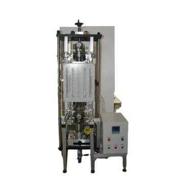
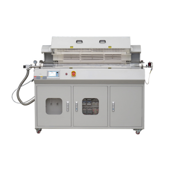
- Customer Made Versatile CVD Tube Furnace Chemical Vapor Deposition Chamber System Equipment
- Split Chamber CVD Tube Furnace with Vacuum Station Chemical Vapor Deposition System Equipment Machine
- 1200℃ Split Tube Furnace with Quartz Tube Laboratory Tubular Furnace
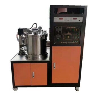
- Vacuum Hot Press Furnace Heated Vacuum Press Machine Tube Furnace
- 1400℃ Laboratory Quartz Tube Furnace with Alumina Tube Tubular Furnace
People Also Ask
- Why are carbon nanotubes important in industry? Unlocking Next-Generation Material Performance
- What are the methods of producing CNT? Scalable CVD vs. High-Purity Lab Techniques
- Are all lab grown diamonds CVD? Understanding the Two Main Methods
- How does chirality affect carbon nanotubes? It Determines If They Are Metal or Semiconductor
- What are nanotubes drawbacks? The 4 Major Hurdles Limiting Their Real-World Use