In essence, thin films are formed by depositing a material, atom by atom or molecule by molecule, onto a surface called a substrate. This entire process occurs within a highly controlled vacuum environment to ensure purity and precision. The two dominant categories of methods for achieving this are Physical Vapor Deposition (PVD) and Chemical Vapor Deposition (CVD).
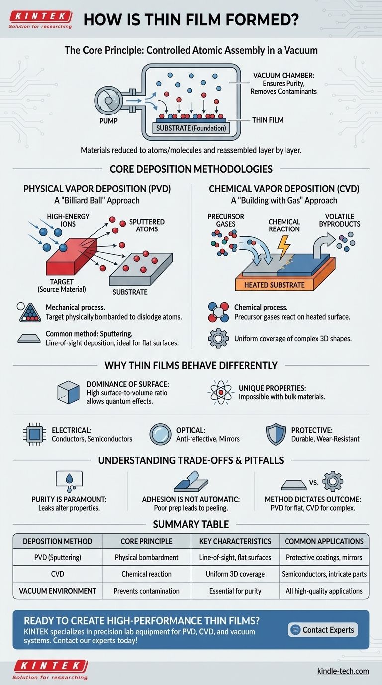
The core principle of thin film formation is the controlled transfer of material from a source to a substrate. By reducing materials to their atomic components and reassembling them in a vacuum, we create layers so thin that their properties differ fundamentally from the bulk material.
The Fundamental Environment: A Controlled Vacuum
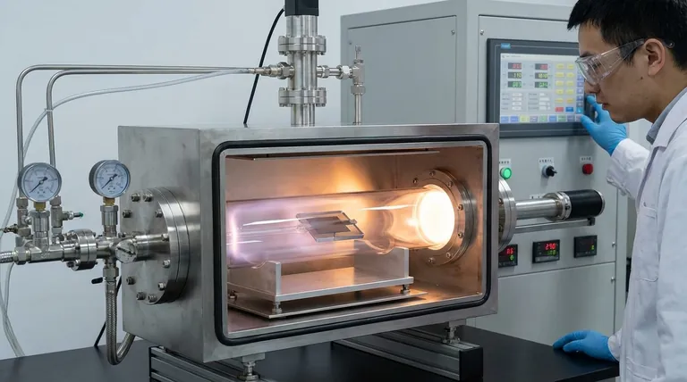
To understand how thin films are made, we must first understand the environment where they are created. The process does not happen in open air; it requires a specialized vacuum chamber.
The Role of the Substrate
The substrate is the foundation. It is the material or object onto which the thin film is deposited. This could be a silicon wafer for an integrated circuit, a piece of glass for a mirror, or a metal tool bit for a protective coating.
The Necessity of a Vacuum
The entire deposition process takes place in a vacuum chamber. Removing air and other gases is critical to prevent the source material from reacting with contaminants before it reaches the substrate. A vacuum ensures the path is clear for a pure, uniform film to form.
Core Deposition Methodologies
While there are many specific techniques, they generally fall into two major categories that describe how the source material is transported to the substrate.
Physical Vapor Deposition (PVD): A "Billiard Ball" Approach
PVD is a mechanical process. The source material, known as a target, is physically bombarded to dislodge atoms.
A common PVD method is sputtering. In this technique, high-energy ions are accelerated towards the target. When these ions strike the target, they knock out, or "sputter," atoms of the source material. These ejected atoms then travel through the vacuum and deposit onto the substrate, gradually building the thin film layer by layer.
Chemical Vapor Deposition (CVD): A "Building with Gas" Approach
CVD is a chemical process. Instead of physically knocking atoms off a solid target, this method introduces precursor gases into the vacuum chamber.
These gases flow over the heated substrate and undergo a chemical reaction directly on its surface. This reaction produces the desired solid material as a film, leaving behind volatile byproducts that are pumped out of the chamber.
Why Thin Films Behave Differently
The reason this complex process is so important is that materials at the thin film scale do not behave like their bulk counterparts.
The Dominance of the Surface
In a thin film, the surface-to-volume ratio is dramatically increased. This means a much higher percentage of atoms are at the surface compared to a solid block of the same material. This change in geometry allows quantum and surface-level effects to dominate the material's overall properties.
Unlocking New Applications
These unique properties are what make thin films so versatile. The process is used to create specific functionalities that are impossible with bulk materials.
- Electrical Films: Used to make the foundational components of all modern electronics, including conductors, insulators, and semiconductors in integrated circuits.
- Optical Films: Precisely engineered to control light, resulting in anti-reflective coatings on eyeglasses, high-reflectivity mirrors, and light-absorbing layers in solar cells.
- Protective Films: Used as extremely adherent and durable thermal or wear-resistant barriers in demanding industries like aerospace.
Understanding the Trade-offs and Pitfalls
Creating a high-quality thin film is a process of extreme precision where small variables have a large impact.
Purity is Paramount
Any unwanted atoms or molecules from a leaky vacuum chamber can become embedded in the film, drastically altering its electrical, optical, or mechanical properties. The pursuit of purer films drove the development of ultra-high vacuum technology.
Adhesion is Not Automatic
While thin films are known for being extremely adherent, this is only true when the process is optimized. Poor substrate preparation or incorrect deposition parameters can lead to a film that peels, cracks, or fails to stick at all.
The Method Dictates the Outcome
The choice between PVD and CVD is not arbitrary. PVD is often a "line-of-sight" process, which is excellent for coating flat surfaces but struggles with complex shapes. CVD, which uses gases, can often coat intricate 3D objects more uniformly. The right choice depends entirely on the desired material and application.
Matching the Process to Your Goal
Your final objective determines which deposition characteristics are most important.
- If your primary focus is creating durable, dense coatings on flat surfaces (like tool bits or optics): A PVD method like sputtering is often the ideal choice due to its direct, physical deposition of atoms.
- If your primary focus is uniformly coating complex 3D shapes or creating high-purity semiconductor layers: CVD is often superior because the precursor gases can reach all surfaces to react and form the film.
- If your primary focus is advanced performance (like in solar cells or next-gen electronics): The key is precise control over the atomic-scale structure, making advanced vacuum and deposition techniques absolutely essential.
Ultimately, understanding these formation principles reveals how manipulating materials at the atomic level engineers the technology of our modern world.
Summary Table:
| Deposition Method | Core Principle | Key Characteristics | Common Applications |
|---|---|---|---|
| PVD (Physical Vapor Deposition) | Physical bombardment of target material | Line-of-sight deposition, excellent for flat surfaces | Protective coatings, mirrors, tool bits |
| CVD (Chemical Vapor Deposition) | Chemical reaction of precursor gases on substrate | Uniform coverage of complex 3D shapes | Semiconductor devices, intricate coatings |
| Vacuum Environment | Prevents contamination and ensures purity | Essential for both PVD and CVD processes | All high-quality thin film applications |
Ready to create high-performance thin films for your laboratory? KINTEK specializes in precision lab equipment and consumables for thin film deposition. Whether you're working with PVD, CVD, or advanced vacuum systems, our solutions ensure the purity, adhesion, and uniformity your research demands. Contact our experts today to discuss how we can support your specific thin film application needs!
Visual Guide
Related Products
- Chemical Vapor Deposition CVD Equipment System Chamber Slide PECVD Tube Furnace with Liquid Gasifier PECVD Machine
- HFCVD Machine System Equipment for Drawing Die Nano-Diamond Coating
- Customer Made Versatile CVD Tube Furnace Chemical Vapor Deposition Chamber System Equipment
- RF PECVD System Radio Frequency Plasma-Enhanced Chemical Vapor Deposition RF PECVD
- Split Chamber CVD Tube Furnace with Vacuum Station Chemical Vapor Deposition System Equipment Machine
People Also Ask
- What types of substrates are used in CVD to facilitate graphene films? Optimize Graphene Growth with the Right Catalyst
- What are the processes of vapor phase deposition? Understand CVD vs. PVD for Superior Thin Films
- What is plasma enhanced chemical vapor deposition PECVD equipment? A Guide to Low-Temperature Thin Film Deposition
- What happens during deposition chemistry? Building Thin Films from Gaseous Precursors
- What are the advantages of chemical vapor deposition? Achieve Superior Thin Films for Your Lab


