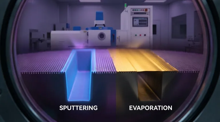
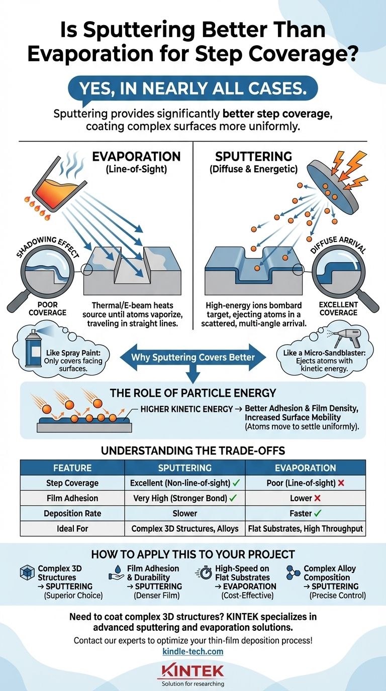
In nearly all cases, yes. Sputtering provides significantly better step coverage than standard thermal or electron-beam evaporation. The fundamental difference in how atoms are ejected from the source and travel to the substrate gives sputtering a distinct advantage in coating complex, non-flat surfaces. Evaporation is a "line-of-sight" process, leading to thin or non-existent films on vertical sidewalls, while sputtering creates a more diffuse vapor that coats surfaces from multiple angles.
The core issue isn't simply which method is "better," but understanding how the physics of each process impacts the final film. Sputtering's superior coverage comes from its scattered, high-energy particle arrival, but this advantage is balanced by a slower deposition rate compared to evaporation.
The Physics of Deposition: Why Sputtering Covers Better
The difference in step coverage is a direct result of how atoms are liberated from the source material and travel to the substrate.
Evaporation: A "Line-of-Sight" Process
In thermal or e-beam evaporation, a source material is heated in a high vacuum until its atoms vaporize and travel in straight lines toward the substrate.
Think of this like using a can of spray paint. The paint only covers the surfaces directly facing the nozzle. Any vertical walls or undercut features will be left in a "shadow" and receive little to no coating. This shadowing effect is why evaporation struggles with step coverage.
Sputtering: A Diffuse, Energetic Arrival
Sputtering does not use heat to vaporize material. Instead, a target of the source material is bombarded by high-energy ions (typically from an inert gas like Argon) in a plasma environment.
This bombardment acts like a microscopic sandblaster, ejecting target atoms with significant kinetic energy. These ejected atoms collide with the surrounding gas particles, causing them to scatter and approach the substrate from a wide range of angles, not just a single straight line.
This diffuse, multi-angle arrival is the primary reason sputtering can effectively coat the sidewalls of trenches and other complex topographies.
The Role of Particle Energy
Sputtered particles arrive at the substrate with much higher energy than evaporated particles. This has two key benefits for coverage.
First, the high energy promotes better adhesion and film density, creating a more robust and durable coating.
Second, this energy allows atoms to move around slightly on the surface after they land—a phenomenon known as surface mobility. This mobility helps the atoms settle into a more uniform and continuous film, further improving coverage over small features.
Understanding the Trade-offs
Choosing sputtering for its step coverage means accepting a series of important trade-offs.
Deposition Rate: Speed vs. Quality
Evaporation is a much faster deposition process. For applications requiring thick films on relatively flat surfaces, evaporation is often the more efficient and economical choice. Sputtering is inherently slower.
Film Properties: Adhesion and Density
Sputtering wins decisively here. The energetic bombardment creates films with adhesion strengths that can be 10 times greater than evaporated films. Sputtered films are also typically denser and harder.
Material and Substrate Considerations
Sputtering offers more precise control over film thickness and uniformity and is excellent for depositing alloys and compounds, as the material composition transfers predictably from the target to the film.
While sputtering can often be performed at lower substrate temperatures than evaporation, the energetic plasma can sometimes cause damage to extremely sensitive substrates.
How to Apply This to Your Project
Your choice ultimately depends on which film properties are most critical for your application's success.
- If your primary focus is excellent step coverage on complex 3D structures: Sputtering is the superior technical choice due to its non-directional deposition.
- If your primary focus is film adhesion and durability: Sputtering provides a significantly denser and more strongly bonded film.
- If your primary focus is high-speed deposition of thick films on flat substrates: E-beam evaporation is often more practical and cost-effective.
- If you are depositing a complex alloy and must preserve its stoichiometry: Sputtering offers better control over the final film's composition.
By understanding the fundamental physics of material arrival, you can confidently select the deposition method that ensures your film's performance and reliability.
Summary Table:
| Feature | Sputtering | Evaporation |
|---|---|---|
| Step Coverage | Excellent (non-line-of-sight) | Poor (line-of-sight) |
| Film Adhesion | Very High | Lower |
| Deposition Rate | Slower | Faster |
| Ideal For | Complex 3D structures, alloys | Flat substrates, high throughput |
Need to coat complex 3D structures with a uniform, durable film?
KINTEK specializes in lab equipment and consumables, providing advanced sputtering and evaporation solutions tailored to your research and production needs. Our expertise ensures you select the right deposition method for superior film adhesion, precise stoichiometry, and reliable performance.
Contact our experts today to discuss how we can optimize your thin-film deposition process!
Visual Guide
Related Products
- Spark Plasma Sintering Furnace SPS Furnace
- Vacuum Induction Melting Spinning System Arc Melting Furnace
- Chemical Vapor Deposition CVD Equipment System Chamber Slide PECVD Tube Furnace with Liquid Gasifier PECVD Machine
- Customer Made Versatile CVD Tube Furnace Chemical Vapor Deposition Chamber System Equipment
People Also Ask
- What is the pressure for spark plasma sintering? A Guide to Optimizing SPS Parameters
- What is the mechanism of SPS process? A Deep Dive into Rapid, Low-Temperature Sintering
- What is the process fundamentals of spark plasma sintering? Achieve Rapid, High-Density Material Consolidation
- What is SPS sintering method? A Guide to High-Speed, High-Performance Material Fabrication
- What are the fundamentals of spark plasma sintering process? Unlock Rapid, High-Performance Material Consolidation


