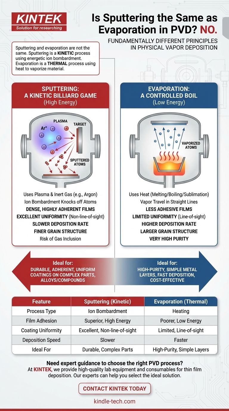
No, sputtering and evaporation are not the same process. Although both are forms of Physical Vapor Deposition (PVD), they operate on fundamentally different principles. Sputtering is a kinetic process that uses energetic ion bombardment to physically eject atoms from a source, while evaporation is a thermal process that uses heat to boil or sublimate a material into a vapor.
The core distinction to remember is this: sputtering produces dense, highly adherent films with superior uniformity, making it ideal for robust applications. Evaporation is generally a faster and purer process, but it produces less adhesive films with "line of sight" coverage limitations.

The Core Difference: A Physical vs. Thermal Process
To understand why these methods produce different results, we must examine their core mechanics. The way atoms leave the source material directly influences their energy, their travel path, and how they ultimately form a film on the substrate.
Sputtering: A Kinetic Billiard Game
Sputtering is best understood as a physical collision process. It begins by creating a plasma in a low-vacuum environment, typically using an inert gas like argon.
These positively charged gas ions are accelerated by an electric field and slam into the source material, known as the target.
This high-energy impact acts like a microscopic billiard break, knocking individual atoms or small clusters off the target surface. These "sputtered" atoms travel through the chamber and condense on the substrate, forming the thin film.
Evaporation: A Controlled Boil
Evaporation is a much simpler thermal concept. In a high-vacuum chamber, the source material is heated until it reaches its vaporization temperature.
As the material melts and then boils (or sublimates directly from solid to gas), it releases a vapor of atoms.
These vaporized atoms travel in a straight line until they encounter a cooler surface, such as the substrate, where they condense back into a solid state, forming a thin layer.
How the Process Dictates Film Properties
The difference between a high-energy atomic collision and a low-energy thermal vapor stream has profound consequences for the quality and characteristics of the final coating.
Film Adhesion and Density
In sputtering, atoms arrive at the substrate with significantly high energy. This energy helps them form a denser, more tightly packed film.
The result is superior adhesion and mechanical durability, as the energetic particles can create a stronger bond with the substrate surface. Evaporated atoms arrive with low thermal energy, leading to poorer adhesion.
Deposition Rate and Speed
Evaporation typically produces a robust vapor stream, enabling much higher deposition rates than sputtering.
This makes evaporation a faster and often more economical process for depositing thick layers of pure metals or simple materials.
Coating Uniformity
Sputtered atoms are ejected from the target and then scatter through the low-pressure gas in the chamber. This scattering effect results in excellent film uniformity, even over complex, non-flat shapes.
Evaporation is a "line-of-sight" process. The vapor travels in a straight line, making it difficult to coat undercuts or the sides of a complex object uniformly without sophisticated substrate manipulation.
Purity and Grain Structure
Because it operates in a high vacuum with no process gas, evaporation can produce films of very high purity. The lower energy of arriving atoms also tends to form larger grain sizes in the film's microstructure.
Sputtering's use of a process gas (like argon) creates a risk of that gas becoming entrapped in the growing film, which can be an impurity. The high energy of sputtered atoms typically results in a finer, smaller grain structure.
Understanding the Trade-offs
Neither method is universally superior; the choice is always dictated by the requirements of the application. Understanding the inherent limitations of each is key to making an informed decision.
The Limitations of Sputtering
The primary drawback of sputtering is its slower deposition rate for many materials, which can increase process time and cost.
Additionally, the process is more complex, requiring high-voltage power supplies and careful control of the plasma environment. There is also a small but notable risk of the process gas being incorporated into the film.
The Weaknesses of Evaporation
The most significant weakness of evaporation is the poor adhesion of the resulting film, making it unsuitable for applications requiring high durability or wear resistance.
Furthermore, its line-of-sight nature severely limits its ability to coat complex geometries uniformly. It is also challenging to evaporate alloys or compounds without altering their chemical composition, as different elements will vaporize at different rates.
Making the Right Choice for Your Application
Selecting the correct PVD method requires aligning the process capabilities with your primary goal for the final film.
- If your primary focus is durability, adhesion, and uniformity: Sputtering is the superior choice for creating dense, hard, and highly adherent coatings on complex parts.
- If your primary focus is deposition speed and film purity: Evaporation is often preferred for quickly depositing simple, high-purity metal layers where adhesion is not the critical factor.
- If your primary focus is coating complex alloys or compounds: Sputtering excels at maintaining the original composition (stoichiometry) of the source material in the final film.
Ultimately, understanding these fundamental differences empowers you to select the precise tool to engineer the exact film your application demands.
Summary Table:
| Feature | Sputtering | Evaporation |
|---|---|---|
| Process Type | Kinetic (Ion Bombardment) | Thermal (Heating) |
| Film Adhesion | Superior, High Energy | Poorer, Low Energy |
| Coating Uniformity | Excellent, non-line-of-sight | Limited, line-of-sight |
| Deposition Speed | Slower | Faster |
| Ideal For | Durable, adherent coatings on complex parts | High-purity, simple metal layers |
Need expert guidance to choose the right PVD process for your specific application?
At KINTEK, we specialize in providing high-quality lab equipment and consumables for all your thin film deposition needs. Whether your project requires the robust, uniform coatings of sputtering or the high-purity, fast deposition of evaporation, our experts can help you select the ideal solution to enhance your research and development.
Contact our team today to discuss your requirements and discover how KINTEK can support your laboratory's success.
Visual Guide
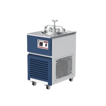
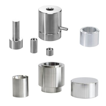
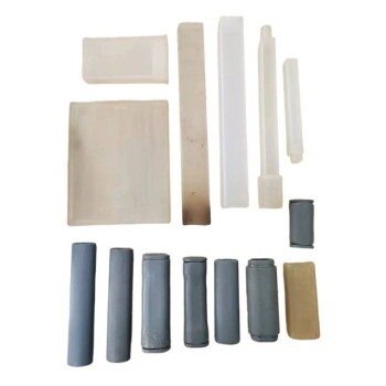
Related Products
- RF PECVD System Radio Frequency Plasma-Enhanced Chemical Vapor Deposition RF PECVD
- Molybdenum Tungsten Tantalum Evaporation Boat for High Temperature Applications
- Chemical Vapor Deposition CVD Equipment System Chamber Slide PECVD Tube Furnace with Liquid Gasifier PECVD Machine
- Hemispherical Bottom Tungsten Molybdenum Evaporation Boat
- Aluminized Ceramic Evaporation Boat for Thin Film Deposition
People Also Ask
- What is an example of PECVD? RF-PECVD for High-Quality Thin Film Deposition
- What are the applications of PECVD? Essential for Semiconductors, MEMS, and Solar Cells
- What is plasma activated chemical vapour deposition method? A Low-Temperature Solution for Advanced Coatings
- How are PECVD and CVD different? A Guide to Choosing the Right Thin-Film Deposition Process
- Why is PECVD environment friendly? Understanding the Eco-Friendly Benefits of Plasma-Enhanced Coating