In short, the properties of a thin film are determined by the materials used to create it and, more critically, the deposition process and specific environmental parameters used during its formation. Factors like substrate temperature, the energy of depositing particles, and the geometry of the deposition system directly control the film's final characteristics.
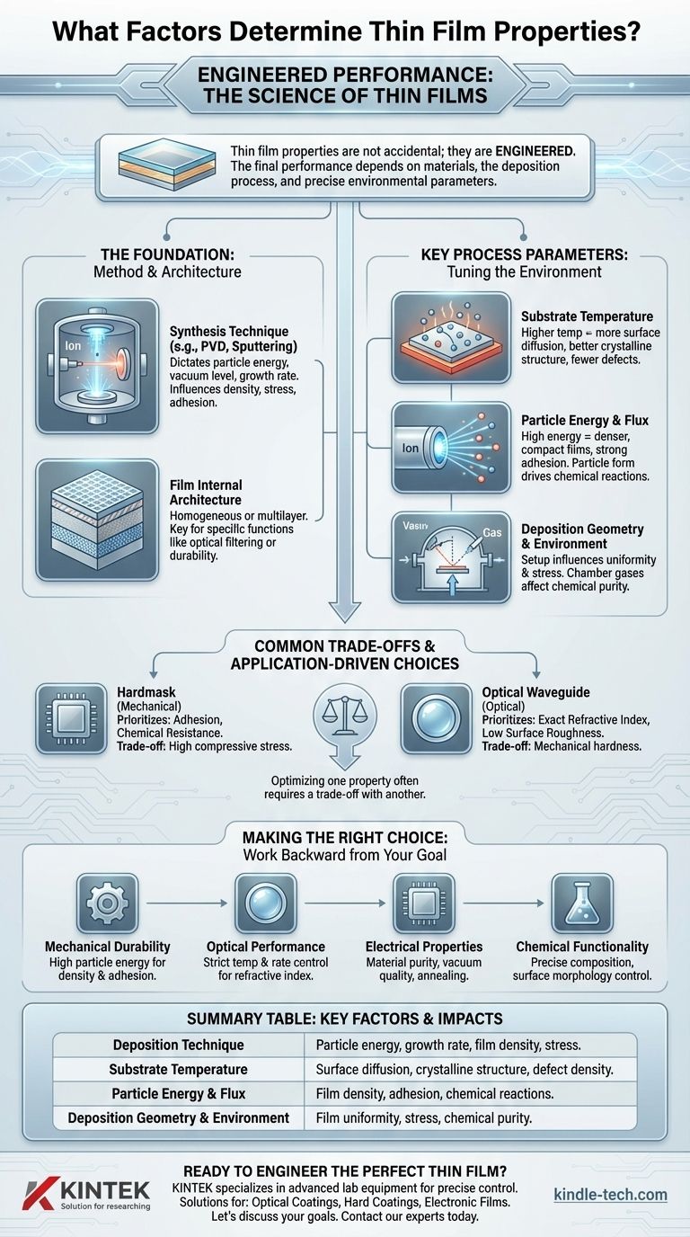
The core principle to understand is that a thin film's properties are not accidental; they are engineered. The final performance—be it optical, mechanical, or electrical—is a direct consequence of the precise and controllable conditions under which the film is grown.
The Foundation: Method and Architecture
Before fine-tuning any process, the two most fundamental choices you will make are the deposition technique and the intended structure of the film. These high-level decisions set the boundaries for the properties you can achieve.
Choosing the Synthesis Technique
The method used to create the film is a primary factor. Techniques like Physical Vapor Deposition (PVD), ion beam sputtering, or magnetron sputtering each operate under different physical principles.
This choice dictates the energy range of the depositing particles, the achievable vacuum level, and the rate of growth, fundamentally influencing the film's density, stress, and adhesion.
The Film's Internal Architecture
A thin film is not always a single, uniform layer. Its properties are heavily dependent on its designed structure.
It can be a homogeneous single layer with a consistent composition or a complex inhomogeneous multilayer structure. This architecture can be periodic, patterned, or random, and it is a key design choice for achieving specific functions like optical filtering or enhanced durability.
Key Process Parameters You Can Control
Once a method is chosen, the specific properties of the film are tuned by manipulating the parameters of the growth environment. These variables give you direct control over the film's resulting structure and performance.
Substrate Temperature
The temperature of the surface on which the film is grown is one of the most critical variables.
Higher temperatures provide more energy to the arriving atoms, allowing them to move around on the surface (surface diffusion). This mobility helps form more ordered, crystalline structures and can reduce internal stress and defects.
Particle Energy and Flux
The energy and rate (flux) of the atoms or ions arriving at the substrate have a profound impact on the film's density.
High-energy particles, common in sputtering processes, can create denser, more compact films with strong adhesion. The form of these particles, such as specific radicals in a plasma, also dictates the chemical reactions that occur on the growing surface.
Deposition Geometry and Environment
The physical setup of the deposition chamber, including the distance and angle between the material source and the substrate (scattering geometry), influences the film's uniformity and stress.
Furthermore, the background pressure and the composition of gases within the chamber can introduce impurities or participate in reactions, altering the film's final chemical and electrical properties.
Common Trade-offs and Application-Driven Choices
There is no single "best" thin film; there is only the right film for a specific application. Understanding this context is crucial, as optimizing for one property often requires a trade-off with another.
A Hardmask vs. an Optical Waveguide
The intended application entirely dictates which properties matter.
A film used as a hardmask for etching requires excellent adhesion and chemical resistance but may not need specific optical or electrical characteristics. Conversely, a film for an optical waveguide demands an exact refractive index and minimal surface roughness, while its mechanical hardness may be a secondary concern.
Optimizing One Property at the Expense of Another
Engineering a film is a balancing act. For instance, processes that create extremely hard and dense coatings often do so by inducing high compressive stress within the film.
This high stress, while beneficial for hardness, can sometimes lead to poor adhesion or cause the film to crack, especially on flexible substrates. You must decide which characteristic is more critical for your goal.
Making the Right Choice for Your Goal
To engineer a film effectively, you must work backward from your desired outcome. Your primary application will determine which deposition parameters to prioritize and control.
- If your primary focus is mechanical durability (e.g., hard coatings): Prioritize deposition methods that deliver high particle energy to maximize film density and adhesion.
- If your primary focus is precise optical performance (e.g., anti-reflection coatings): Focus on strict control over substrate temperature and deposition rate to fine-tune the refractive index and minimize light scattering from surface roughness.
- If your primary focus is specific electrical properties (e.g., microelectronics): Pay close attention to material purity, vacuum quality, and post-deposition annealing to control the film's crystalline structure and purity.
- If your primary focus is chemical functionality (e.g., sensors or catalysts): Choose methods that allow for precise compositional control and can create a specific surface morphology, such as high porosity.
Ultimately, creating a thin film is an act of deliberate engineering, where every parameter is a lever to achieve a desired outcome.
Summary Table:
| Key Factor | Impact on Thin Film Properties |
|---|---|
| Deposition Technique | Determines particle energy, growth rate, and achievable film density and stress. |
| Substrate Temperature | Controls surface diffusion, influencing crystalline structure and defect density. |
| Particle Energy & Flux | Affects film density, adhesion, and the chemical reactions during growth. |
| Deposition Geometry & Environment | Influences film uniformity, stress, and chemical purity. |
Ready to engineer the perfect thin film for your application?
The properties of your thin film—whether for optical, mechanical, or electrical performance—are a direct result of the deposition process. At KINTEK, we specialize in providing the advanced lab equipment and expert support needed to precisely control these critical parameters.
We serve laboratories focused on R&D and production, offering solutions for:
- Optical Coatings: Achieve precise refractive index and low surface roughness.
- Hard Coatings: Maximize density and durability for demanding environments.
- Electronic Films: Ensure high purity and specific crystalline structures.
Let's discuss your specific goals. Contact our experts today to find the ideal deposition solution for your project.
Visual Guide
Related Products
- Aluminized Ceramic Evaporation Boat for Thin Film Deposition
- Tungsten Evaporation Boat for Thin Film Deposition
- Electron Beam Evaporation Coating Oxygen-Free Copper Crucible and Evaporation Boat
- Molybdenum Tungsten Tantalum Evaporation Boat for High Temperature Applications
- HFCVD Machine System Equipment for Drawing Die Nano-Diamond Coating
People Also Ask
- What are the applications of thin films deposition? Unlock New Possibilities for Your Materials
- What are the alternatives to sputtering? Choose the Right Thin Film Deposition Method
- Why is an alumina boat selected for catalyst precursors? Ensure Sample Purity at 1000 °C
- What are thin films deposited by evaporation? A Guide to High-Purity Coating
- Why is an alumina boat and Ti3AlC2 powder bed necessary for Ti2AlC sintering? Protect MAX Phase Purity


