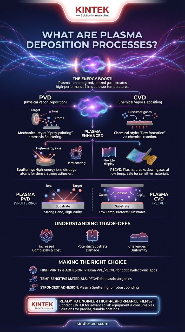
In short, plasma deposition is not a single technique but a category of advanced processes that use plasma—an energized, ionized gas—to create high-performance thin films. These methods fall under the two primary families of deposition, Physical Vapor Deposition (PVD) and Chemical Vapor Deposition (CVD), but use the unique properties of plasma to achieve results not possible with heat alone.
The core takeaway is that using plasma provides the necessary energy to deposit durable, high-quality films at significantly lower temperatures. This makes it possible to coat sensitive materials, like plastics or complex electronics, that would be damaged by traditional high-temperature methods.
The Foundation: PVD vs. CVD
To understand where plasma fits, you must first understand the two foundational pillars of film deposition. Nearly every process is a variation of one of these two approaches.
Physical Vapor Deposition (PVD)
PVD is a mechanical-style process. It involves physically transporting material from a source (called a "target") to the surface you want to coat (the "substrate") inside a vacuum chamber.
Think of it like spray-painting, but instead of paint particles, you are transporting individual atoms or molecules. Common methods include using heat to evaporate the source material or using ion bombardment (sputtering) to knock atoms off the target.
Chemical Vapor Deposition (CVD)
CVD is a chemical-style process. Instead of physically moving a solid material, it involves introducing precursor gases into a chamber.
These gases react on the hot substrate surface, building the desired film layer by layer. It’s analogous to how dew forms on a cool surface, except in this case, a chemical reaction forms a permanent, solid film.
Where Plasma Fits In: An Energy Boost
Plasma is the key that unlocks higher performance and greater versatility for both PVD and CVD. It acts as a highly efficient medium for transferring energy to the deposition process.
The Role of Plasma
A plasma is created by applying energy (typically an electric field) to a neutral gas, causing it to ionize. This "fourth state of matter" is a soup of charged ions, electrons, and neutral particles.
The temperature, density, and chemical composition of this plasma are critical variables. By controlling them, engineers can precisely tune the energy and reactive species involved in the film's creation.
Enhancing PVD with Plasma (Sputtering)
Sputtering is the most common form of plasma-enhanced PVD. In this process, the plasma is used to create high-energy ions.
These ions are accelerated toward the source material target, striking it with enough force to dislodge atoms. These "sputtered" atoms then travel through the vacuum and deposit onto the substrate, forming a dense and strongly adhered film.
Enhancing CVD with Plasma (PECVD)
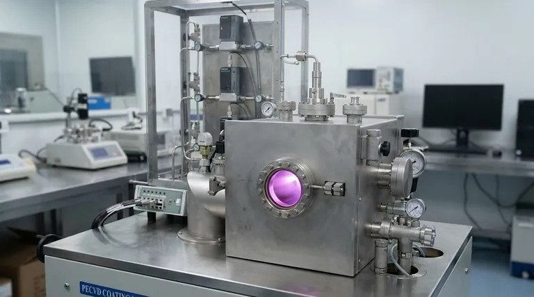
Plasma-Enhanced Chemical Vapor Deposition (PECVD) uses a plasma to break down precursor gases far more efficiently than heat alone.
The plasma's energy creates highly reactive chemical fragments that can form a high-quality film on the substrate at much lower temperatures than conventional CVD. This is essential for modern electronics manufacturing.
Understanding the Trade-offs
While powerful, plasma deposition is not a universal solution. It involves a clear set of trade-offs that are critical to understand before choosing a process.
Increased Complexity and Cost
Generating and controlling a stable plasma requires sophisticated equipment, including power supplies and vacuum systems. This makes plasma-based systems inherently more complex and expensive than simple thermal deposition methods.
Potential for Substrate Damage
The same high-energy ions that are beneficial for sputtering can also cause damage to delicate substrates, such as sensitive electronic components or polymer layers, if the process is not meticulously controlled.
Challenges in Uniformity
Achieving a perfectly uniform plasma density and temperature over a large substrate area is a significant engineering challenge. Non-uniformity can lead to variations in the thickness and properties of the deposited film.
Making the Right Choice for Your Goal
Selecting the right deposition technique requires aligning the process capabilities with the material requirements and substrate limitations of your specific application.
- If your primary focus is high-purity, dense films for demanding optical or electronic applications: Plasma-enhanced processes like sputtering (PVD) or PECVD are the superior choice for their control over film properties.
- If your primary focus is coating temperature-sensitive materials like plastics or organics: Plasma-Enhanced CVD (PECVD) is often the only viable option, as its low process temperature prevents substrate damage.
- If your primary focus is achieving the strongest possible film adhesion: Plasma sputtering is exceptional because the high-energy atoms embed themselves slightly into the substrate surface, creating an incredibly strong bond.
Ultimately, understanding the role of plasma transforms deposition from a simple coating technique into a precise tool for engineering material properties at the atomic scale.
Summary Table:
| Process Type | Key Feature | Common Applications |
|---|---|---|
| Plasma PVD (Sputtering) | High-energy atom deposition for strong adhesion | Optical coatings, wear-resistant surfaces |
| Plasma CVD (PECVD) | Low-temperature deposition for sensitive substrates | Electronics, flexible displays, medical devices |
| Trade-offs | Higher complexity and cost vs. superior film quality | Requires precise control to avoid substrate damage |
Ready to engineer high-performance thin films for your sensitive materials? KINTEK specializes in advanced lab equipment and consumables for plasma deposition processes like PECVD and sputtering. Our solutions help you achieve precise, durable coatings without damaging temperature-sensitive substrates. Contact our experts today to discuss how we can support your laboratory's deposition needs!
Visual Guide
Related Products
- Chemical Vapor Deposition CVD Equipment System Chamber Slide PECVD Tube Furnace with Liquid Gasifier PECVD Machine
- 915MHz MPCVD Diamond Machine Microwave Plasma Chemical Vapor Deposition System Reactor
- RF PECVD System Radio Frequency Plasma-Enhanced Chemical Vapor Deposition RF PECVD
- Microwave Plasma Chemical Vapor Deposition MPCVD Machine System Reactor for Lab and Diamond Growth
- Cylindrical Resonator MPCVD Machine System Reactor for Microwave Plasma Chemical Vapor Deposition and Lab Diamond Growth
People Also Ask
- What are the processes of vapor phase deposition? Understand CVD vs. PVD for Superior Thin Films
- What types of substrates are used in CVD to facilitate graphene films? Optimize Graphene Growth with the Right Catalyst
- How are carbon nanotubes grown? Master Scalable Production with Chemical Vapor Deposition
- What are the core advantages of PE-CVD in OLED encapsulation? Protect Sensitive Layers with Low-Temp Film Deposition
- Why is Chemical Vapor Deposition (CVD) equipment uniquely suited for constructing hierarchical superhydrophobic structures?


