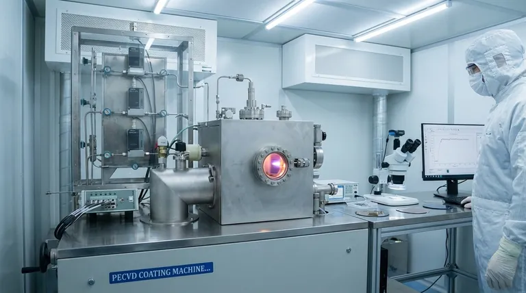
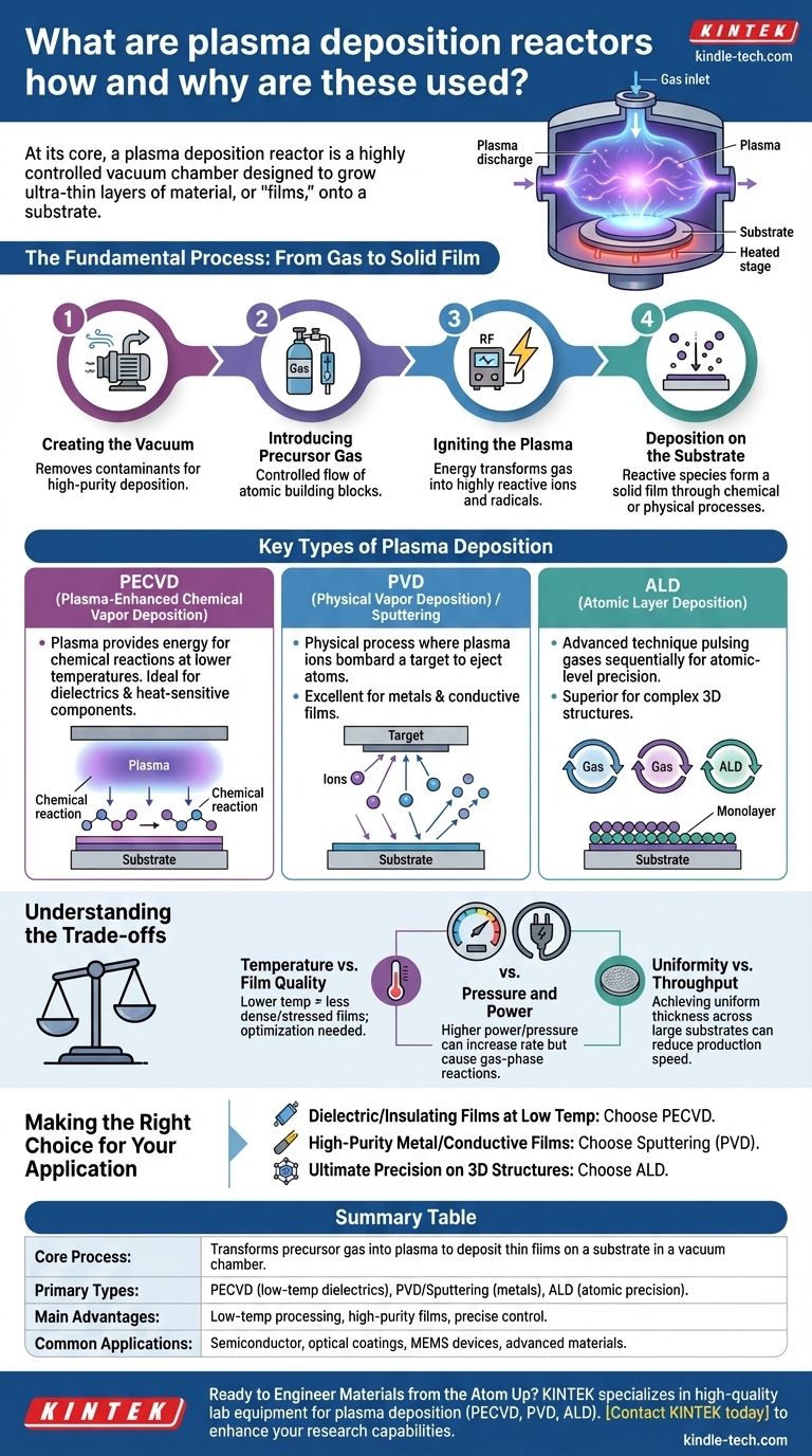
At its core, a plasma deposition reactor is a highly controlled vacuum chamber designed to grow ultra-thin layers of material, or "films," onto a surface, known as a substrate. It achieves this by transforming a precursor gas into an energized state of matter called plasma. The reactive particles within this plasma then settle on the substrate, building a solid film with precisely engineered properties, a process fundamental to manufacturing modern electronics, optics, and advanced materials.
Plasma deposition is not merely a coating technique; it is a foundational tool of nanotechnology. It enables the creation of high-performance materials from the atom up, allowing for deposition at low temperatures that are critical for building complex, multi-layered devices like computer chips.
The Fundamental Process: From Gas to Solid Film
To understand why plasma reactors are so powerful, you must first understand their core operational sequence. The entire process is a carefully choreographed series of physical and chemical events occurring within a sealed environment.
Creating the Vacuum
The process begins by pumping nearly all the air out of the reactor chamber. This vacuum is critical because it removes unwanted atmospheric gases and water vapor, which would otherwise contaminate the film and interfere with the process. A clean, controlled environment is paramount for high-purity deposition.
Introducing the Precursor Gas
Next, one or more precursor gases are introduced into the chamber at a precisely controlled flow rate. These gases contain the atomic building blocks of the desired film. For example, to deposit a silicon nitride film, gases like silane (SiH₄) and ammonia (NH₃) might be used.
Igniting the Plasma: The Fourth State of Matter
With the precursor gas inside, energy—typically in the form of a radio frequency (RF) or direct current (DC) electrical field—is applied to the chamber. This powerful energy field strips electrons from the gas atoms and molecules, creating a glowing, highly reactive "soup" of ions, electrons, free radicals, and neutral particles. This is plasma.
Deposition on the Substrate
The highly reactive species within the plasma are then driven toward the substrate. Depending on the specific technique, they either undergo a chemical reaction directly on the substrate's surface to form a new solid material (PECVD) or physically bombard a target to knock atoms loose, which then land on the substrate (PVD).
Key Types of Plasma Deposition
While the core principle remains the same, different reactor types leverage the plasma in distinct ways to achieve different outcomes.
PECVD (Plasma-Enhanced Chemical Vapor Deposition)
In PECVD, the plasma's primary role is to provide the energy needed to break down precursor gases and drive chemical reactions on the substrate surface. This "plasma enhancement" allows high-quality films to be deposited at much lower temperatures than in traditional Chemical Vapor Deposition (CVD), which relies solely on high heat. This is crucial for coating heat-sensitive electronic components.
PVD (Physical Vapor Deposition) / Sputtering
In PVD, the process is physical rather than chemical. A plasma of an inert gas, such as Argon, is created. The positive Argon ions are accelerated into a solid block of source material, called the "target." This energetic bombardment acts like an atomic-scale sandblaster, knocking atoms off the target, which then travel across the chamber and deposit onto the substrate, forming a thin film.
ALD (Atomic Layer Deposition)
ALD is a more advanced technique that provides the ultimate level of precision. It uses a sequence of self-limiting chemical reactions, where precursor gases are pulsed into the chamber one at a time. This process builds the material literally one atomic layer per cycle, resulting in unparalleled uniformity and the ability to perfectly coat highly complex, three-dimensional structures.
Understanding the Trade-offs
Plasma deposition is a powerful technology, but it involves critical engineering trade-offs. The quality of the final film is a direct result of balancing competing process parameters.
Temperature vs. Film Quality
A key advantage of plasma is low-temperature processing. However, films deposited at lower temperatures can sometimes be less dense or have more internal stress compared to those grown at higher temperatures. Optimizing the plasma can help mitigate this, but the trade-off remains a core consideration.
Pressure and Power
The chamber pressure and the amount of power used to generate the plasma are directly linked. Higher power and pressure can increase the deposition rate but may also lead to gas-phase reactions that create particles, contaminating the film. They also influence the film's stress and density.
Uniformity vs. Throughput
Achieving a perfectly uniform film thickness across a large substrate (like a 300mm silicon wafer) is a significant challenge. Reactor designs and process recipes are often optimized to favor uniformity, but this can come at the cost of a slower deposition rate, which reduces manufacturing throughput.
Making the Right Choice for Your Application
Selecting the correct plasma deposition method depends entirely on the material you are creating and its intended function.
- If your primary focus is depositing dielectric or insulating films at low temperatures: PECVD is your go-to method for its balance of speed and quality in applications like semiconductor passivation layers.
- If your primary focus is depositing high-purity metal or conductive films: Sputtering (a form of PVD) offers excellent film purity and adhesion, making it ideal for creating electrical contacts and reflective coatings.
- If your primary focus is achieving ultimate precision and conformal coating on complex 3D structures: ALD is the superior choice for advanced microelectronics and MEMS, despite its slower deposition rate.
By understanding these principles, the reactor is transformed from a complex machine into a precise instrument for engineering materials from the atom up.
Summary Table:
| Key Feature | Description |
|---|---|
| Core Process | Transforms precursor gas into plasma to deposit thin films on a substrate in a vacuum chamber. |
| Primary Types | PECVD (low-temperature dielectrics), PVD/Sputtering (metals), ALD (atomic-level precision). |
| Main Advantages | Low-temperature processing, high-purity films, precise control over material properties. |
| Common Applications | Semiconductor manufacturing, optical coatings, MEMS devices, advanced material research. |
Ready to Engineer Materials from the Atom Up?
Plasma deposition is the cornerstone of modern nanotechnology, enabling the creation of high-performance thin films for semiconductors, optics, and advanced materials. KINTEK specializes in providing high-quality lab equipment and consumables for plasma deposition processes, including PECVD, PVD, and ALD systems. Whether you're developing next-generation electronics or conducting cutting-edge materials research, our expertise ensures you have the precise tools needed for success.
Contact KINTEK today to discuss your specific laboratory needs and discover how our solutions can enhance your research and development capabilities.
Visual Guide
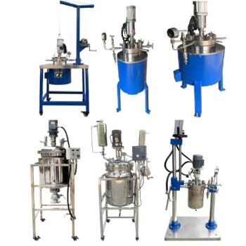
Related Products
- Microwave Plasma Chemical Vapor Deposition MPCVD Machine System Reactor for Lab and Diamond Growth
- 915MHz MPCVD Diamond Machine Microwave Plasma Chemical Vapor Deposition System Reactor
- Cylindrical Resonator MPCVD Machine System Reactor for Microwave Plasma Chemical Vapor Deposition and Lab Diamond Growth
- Chemical Vapor Deposition CVD Equipment System Chamber Slide PECVD Tube Furnace with Liquid Gasifier PECVD Machine
- RF PECVD System Radio Frequency Plasma-Enhanced Chemical Vapor Deposition RF PECVD
People Also Ask
- Why is argon-rich gas phase chemistry used for UNCD growth? Unlock Precision Nano-Diamond Synthesis
- What are the advantages of a Microwave Plasma CVD reactor for MCD/NCD coatings? Precision Multilayer Diamond Engineering
- How does a microwave plasma reactor facilitate the synthesis of diamond? Master MPCVD with Precision Technology
- What pressure is needed for chemical vapor deposition of diamonds? Master the Low-Pressure 'Sweet Spot'
- How are CVD diamonds created? Discover the Science of Lab-Grown Diamond Precision