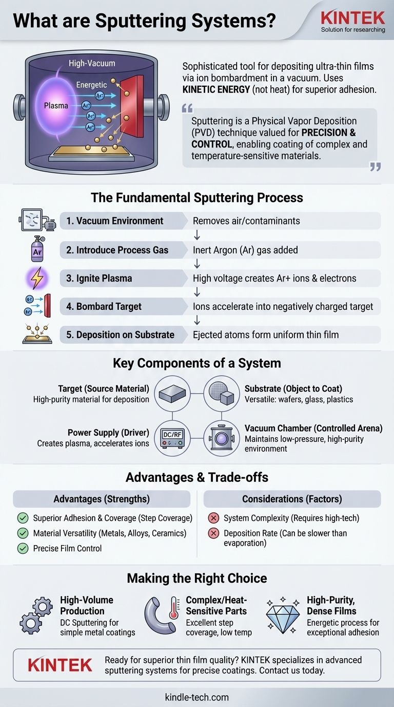
At its core, a sputtering system is a sophisticated tool for depositing ultra-thin films of material onto a surface. It operates within a high-vacuum chamber by using a plasma to generate energetic ions. These ions are accelerated into a source material, known as a "target," bombarding it with enough force to eject, or "sputter," individual atoms. These liberated atoms then travel and deposit onto a component, the "substrate," forming a highly uniform and adherent thin film.
Sputtering is a physical vapor deposition (PVD) technique valued for its precision and control. Unlike methods that melt material, sputtering uses kinetic energy—not heat—to transfer atoms from a solid source. This fundamental difference results in superior film adhesion and the ability to coat complex materials, including temperature-sensitive plastics.
The Fundamental Sputtering Process: From Plasma to Film
To understand a sputtering system, you must first understand its core process. It is a sequence of precise physical events that occur within a highly controlled environment.
Creating the Vacuum Environment
The entire process must occur in a vacuum chamber. This is critical to remove air and other unwanted gas molecules that could react with or contaminate the film being created.
Introducing the Process Gas
Once a vacuum is achieved, a small, controlled amount of an inert process gas—most commonly argon (Ar)—is introduced into the chamber. This gas does not chemically react with the target material; its purpose is purely physical.
Igniting the Plasma
A high voltage is applied within the chamber, typically creating a strong negative charge on the target material. This electrical potential energizes the chamber, stripping electrons from the argon atoms and creating a glowing, ionized gas known as a plasma. This plasma consists of positively charged argon ions (Ar+) and free electrons.
Bombarding the Target
The positively charged argon ions are forcefully accelerated toward the negatively charged target. They collide with the target surface with significant kinetic energy.
Deposition onto the Substrate
This high-energy impact physically knocks atoms loose from the target material. These sputtered atoms travel through the vacuum and land on the substrate, which is strategically placed to intercept them. Atom by atom, a thin film builds up on the substrate's surface.
Key Components of a Sputtering System
Every sputtering system, regardless of its specific type, relies on a few critical components to function.
The Target: The Source Material
The target is a solid block or plate of the material you wish to deposit. It is bonded to a holder, which often includes water cooling channels to manage the heat generated during ion bombardment. The quality of this material is paramount, as any impurities or cracks can lead to a contaminated or defective film.
The Substrate: The Object to be Coated
This is the component receiving the thin film. A key advantage of sputtering is its versatility; substrates can range from silicon wafers and glass panels to heat-sensitive plastics and complex 3D parts.
The Power Supply: Driving the Process
The power supply is what creates the plasma and accelerates the ions. The most straightforward type is a Direct Current (DC) supply. DC sputtering is highly effective and cost-efficient for depositing electrically conductive materials like pure metals.
The Vacuum Chamber: A Controlled Arena
The chamber and its associated pumps provide the essential vacuum environment. The ability to maintain a very low pressure (e.g., 1 to 100 mTorr) is what enables the high-purity deposition process.
Understanding the Key Advantages and Trade-offs
Sputtering is chosen for specific reasons. Understanding its strengths and inherent considerations is key to deciding if it's the right process for a given application.
Advantage: Superior Adhesion and Coverage
The sputtered atoms arrive at the substrate with high kinetic energy. This energy helps them form a denser, more strongly bonded film than is possible with lower-energy processes. It also allows the atoms to coat complex, non-flat surfaces with excellent uniformity, a trait known as step coverage.
Advantage: Material Versatility and Control
Sputtering can deposit pure metals, alloys, and—with more advanced power supplies like Radio Frequency (RF)—electrically insulating ceramic materials. The film thickness is precisely controlled by managing the deposition time and power, ensuring high reproducibility from one run to the next.
Consideration: System Complexity
Sputtering systems are sophisticated pieces of equipment. They require high-vacuum technology, high-voltage power supplies, and careful process control, making them more complex than simple chemical or thermal coating methods.
Consideration: Deposition Rate
While DC sputtering can achieve high deposition rates for certain pure metals, the process can be slower than thermal evaporation for other materials. The primary value of sputtering often lies in film quality rather than raw speed.
Making the Right Choice for Your Application
Choosing a deposition technology depends entirely on your end goal. Sputtering excels in applications where film quality, adhesion, and precision are the dominant requirements.
- If your primary focus is high-volume production of simple metal coatings: DC sputtering is a proven, cost-effective, and high-throughput solution.
- If your primary focus is coating complex 3D parts or heat-sensitive materials: Sputtering's excellent step coverage and low substrate temperature make it a superior choice.
- If your primary focus is creating high-purity, dense films with exceptional adhesion: The energetic nature of the sputtering process provides film qualities that are difficult to achieve with other methods.
Ultimately, understanding the principles of sputtering empowers you to select a deposition technology that meets the precise demands of your material and performance goals.
Summary Table:
| Component | Function | Key Feature |
|---|---|---|
| Target | Source material for deposition | High-purity solid block or plate |
| Substrate | Object receiving the coating | Versatile (wafers, glass, plastics, 3D parts) |
| Vacuum Chamber | Provides controlled environment | Enables high-purity, contamination-free deposition |
| Power Supply | Creates plasma and accelerates ions | DC for metals, RF for insulating materials |
Ready to achieve superior thin film quality for your lab? KINTEK specializes in advanced sputtering systems and lab equipment, delivering precise, uniform coatings for applications ranging from semiconductor manufacturing to medical devices. Our solutions ensure excellent film adhesion, material versatility, and process control. Contact us today to discuss how our expertise can enhance your deposition process and meet your specific laboratory needs.
Visual Guide
Related Products
- Spark Plasma Sintering Furnace SPS Furnace
- Vacuum Induction Melting Spinning System Arc Melting Furnace
- Chemical Vapor Deposition CVD Equipment System Chamber Slide PECVD Tube Furnace with Liquid Gasifier PECVD Machine
- Customer Made Versatile CVD Tube Furnace Chemical Vapor Deposition Chamber System Equipment
People Also Ask
- What is the pressure for spark plasma sintering? A Guide to Optimizing SPS Parameters
- What are the advantages of CAMI/SPS for W-Cu composite preparation? Reduce cycles from hours to seconds.
- What is the difference between spark plasma sintering and flash sintering? A Guide to Advanced Sintering Methods
- Why are Spark Plasma Sintering (SPS) furnaces or hot presses utilized in the preparation of Li3PS4 solid electrolytes?
- What is the theory of spark plasma sintering? A Guide to Rapid, Low-Temperature Densification


