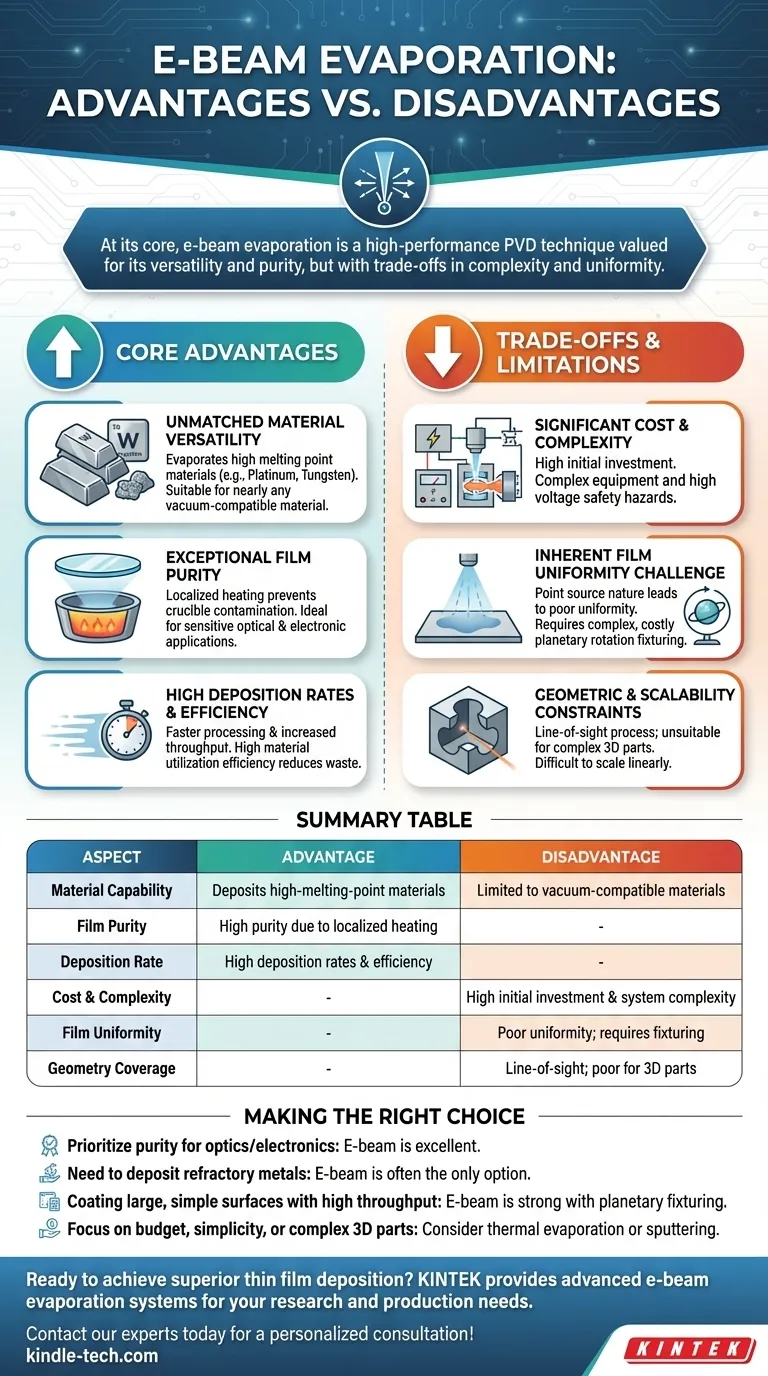
At its core, electron beam (e-beam) evaporation is a high-performance physical vapor deposition (PVD) technique valued for its versatility and purity. It excels at depositing high-quality thin films from a vast range of materials, including those with very high melting points. However, this capability comes with significant trade-offs in equipment complexity, cost, and the inherent challenge of achieving film uniformity.
E-beam evaporation is the preferred method when material purity and the ability to deposit refractory materials are critical. Its primary disadvantages are the high initial investment and the engineering required to overcome its line-of-sight, non-uniform deposition pattern.
The Core Advantages of E-Beam Evaporation
E-beam evaporation offers distinct benefits that make it indispensable for demanding applications, particularly in the optics and semiconductor industries.
Unmatched Material Versatility
The process uses a focused beam of electrons to heat the source material, allowing it to reach extremely high temperatures. This means it can evaporate materials with very high melting points, such as platinum or tungsten, which are impossible to deposit using simpler thermal evaporation methods.
This makes e-beam suitable for nearly any vacuum-compatible material that does not decompose when heated.
Exceptional Film Purity
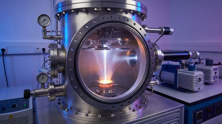
A key advantage is the localized heating. The electron beam heats only the surface of the source material in the crucible, leaving the crucible itself relatively cool.
This prevents contamination from the crucible material leaching into the vapor stream, resulting in exceptionally high-purity thin films. This is a critical factor for sensitive optical and electronic applications.
High Deposition Rates and Efficiency
Compared to other PVD methods like sputtering, e-beam evaporation can achieve significantly higher deposition rates. This allows for faster processing times and increased throughput in production environments.
It also generally offers high material utilization efficiency, meaning more of the source material ends up on the substrate, reducing waste and long-term cost.
Understanding the Trade-offs and Limitations
While powerful, e-beam evaporation is not a universal solution. Its disadvantages are significant and must be carefully considered.
Significant Cost and Complexity
The primary barrier to entry is the equipment itself. E-beam systems require a high-power electron gun, complex magnetic optics for beam steering, and a high-voltage power supply.
This makes the initial investment far more expensive than thermal evaporation systems. The high voltage also introduces a notable safety hazard that requires proper protocols.
The Inherent Challenge of Film Uniformity
E-beam evaporation acts as a "point source," meaning vapor emanates from a small spot and expands outward. This naturally leads to poor film uniformity across a large substrate.
Achieving uniformity requires complex and costly substrate holders with planetary rotation, which move the substrates in a compound motion to average out the deposition. Masks are also often required to fine-tune the coating distribution.
Geometric and Scalability Constraints
As a line-of-sight process, e-beam evaporation is not suitable for coating the inner surfaces of complex, three-dimensional shapes. The vapor can only deposit on surfaces directly visible to the source.
Furthermore, the process is difficult to scale linearly. Simply increasing the power does not always translate to a predictable increase in deposition rate or area, posing challenges for process development and some large-scale applications.
Making the Right Choice for Your Goal
Selecting the right deposition method depends entirely on your project's specific priorities.
- If your primary focus is the highest possible film purity for optics or electronics: E-beam is an excellent choice, as its localized heating minimizes contamination.
- If your primary focus is depositing high-melting-point or refractory metals: E-beam is often the only viable PVD option and is the clear industry standard.
- If your primary focus is coating large, simple surfaces with high throughput: E-beam is a strong candidate, provided you invest in a system with the necessary planetary fixturing to ensure uniformity.
- If your primary focus is budget, simplicity, or coating complex 3D parts: You should strongly consider alternative methods like thermal evaporation for simplicity or sputtering for superior step coverage on complex geometries.
Ultimately, selecting e-beam evaporation is a strategic decision to prioritize film quality and material flexibility over simplicity and initial cost.
Summary Table:
| Aspect | Advantage | Disadvantage |
|---|---|---|
| Material Capability | Deposits high-melting-point materials (e.g., Tungsten) | Limited to vacuum-compatible materials |
| Film Purity | High purity due to localized heating | - |
| Deposition Rate | High deposition rates and material efficiency | - |
| Cost & Complexity | - | High initial investment and system complexity |
| Film Uniformity | - | Poor uniformity; requires planetary fixturing |
| Geometry Coverage | - | Line-of-sight process; poor for 3D parts |
Ready to achieve superior thin film deposition?
At KINTEK, we specialize in providing advanced lab equipment, including e-beam evaporation systems, to meet your most demanding research and production needs. Our expertise ensures you get the right solution for high-purity coatings, refractory materials, and efficient processing.
Let's discuss your project requirements and find the perfect deposition system for you.
Contact our experts today for a personalized consultation!
Visual Guide
Related Products
- Electron Beam Evaporation Coating Oxygen-Free Copper Crucible and Evaporation Boat
- Electron Beam Evaporation Coating Tungsten Crucible and Molybdenum Crucible for High Temperature Applications
- Electron Beam Evaporation Coating Gold Plating Tungsten Molybdenum Crucible for Evaporation
- E Beam Crucibles Electron Gun Beam Crucible for Evaporation
- Electron Beam Evaporation Coating Conductive Boron Nitride Crucible BN Crucible
People Also Ask
- How is an electron beam evaporator cooled during deposition? Essential Thermal Management for Stable Processes
- What is the container that holds the metal source material called in e-beam evaporation? Ensure Purity and Quality in Your Thin-Film Deposition
- What is e-beam evaporation? Achieve High-Purity Thin Film Deposition for Your Lab
- What is the current of e-beam evaporation? A Guide to High-Purity Thin Film Deposition
- What are the applications of electron beams? From Nanoscale Imaging to Industrial Manufacturing


