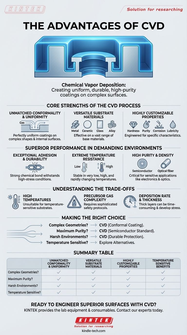
In essence, Chemical Vapor Deposition (CVD) excels at creating highly uniform, durable, and high-purity coatings on a wide variety of materials, even those with complex shapes and internal surfaces. Its key advantages stem from its non-line-of-sight nature, where a precursor gas can reach and react on every exposed surface of a substrate, ensuring a perfectly conformal layer with customizable properties.
The true power of CVD is its ability to engineer surfaces at a molecular level. It is not just a coating method; it is a fabrication process that builds functional, high-performance films with exceptional uniformity on even the most intricate components, a feat that line-of-sight methods cannot achieve.
The Core Strengths of the CVD Process
CVD is chosen when the performance and integrity of the coating are paramount. Its advantages are not isolated benefits but a combination of factors that enable the production of superior films for demanding applications.
Unmatched Conformality and Uniformity
Unlike line-of-sight processes like Physical Vapor Deposition (PVD), CVD is not restricted by geometry. The precursor gas flows into the deposition chamber and surrounds the substrate entirely.
This allows the gas to penetrate internal cavities, sharp corners, and complex surface features, resulting in a perfectly uniform and conformal coating. This is critical for parts like semiconductor wafers, medical implants, and precision engine components.
Versatility in Substrate Materials
CVD is not limited to a single type of base material. The process can be adapted to apply coatings to a vast range of substrates.
This includes metals, metal alloys, ceramics, and even glass. This flexibility makes it a valuable tool across many industries, from aerospace to electronics.
Highly Customizable Film Properties
The final properties of the coating are determined by the chemistry of the precursor gas. This gives engineers immense control over the outcome.
By selecting or optimizing the gas, the resulting film can be engineered for specific characteristics such as high purity, extreme hardness, chemical inertness, corrosion resistance, or high lubricity.
Superior Performance in Demanding Environments
A key reason for selecting CVD is its ability to produce coatings that survive and perform in harsh conditions where other coatings would fail.
Exceptional Adhesion and Durability
The CVD process forms a strong, durable chemical bond between the coating and the substrate material.
This ensures the coating remains intact and functional even in high-stress environments or when the underlying substrate flexes, bends, or experiences vibration.
Extreme Temperature Resistance
CVD coatings are known for their excellent thermal stability.
They can withstand exposure to both very low and very high temperatures, as well as extreme and rapid temperature variations, without degrading or delaminating from the substrate.
High Purity and Density
The process is capable of producing films with exceptionally high purity and density.
This characteristic is non-negotiable in applications like manufacturing semiconductors and optical fibers, where even minuscule impurities can cause catastrophic failure.
Understanding the Trade-offs
While powerful, CVD is not a universal solution. Understanding its inherent characteristics is crucial for making an informed decision. The primary trade-off is the process environment itself.
The Requirement of High Temperatures
CVD is fundamentally an elevated-temperature process, often requiring the substrate to be heated significantly to drive the necessary chemical reactions.
This can be a major limitation, as it makes the process unsuitable for temperature-sensitive substrates like certain polymers or pre-tempered metal alloys that would be damaged by the heat.
Precursor Gas Complexity
The source materials for CVD are reactive gases, which can be toxic, corrosive, or flammable.
Handling these precursors requires sophisticated safety protocols and equipment, adding to the complexity and cost of the process.
Deposition Rate and Thickness
While theoretically capable of building very thick layers, the deposition rate can be a practical constraint.
Building up a thick coating can be time-consuming and expensive. Furthermore, very thick films can sometimes develop internal stresses that may compromise performance, requiring careful process control.
Making the Right Choice for Your Application
Selecting a deposition technology depends entirely on your project's primary objective. CVD offers specific solutions for distinct engineering challenges.
- If your primary focus is coating complex internal geometries: CVD is the superior choice due to its non-line-of-sight, conformal coating capability.
- If your primary focus is achieving maximum film purity for electronics: CVD is the industry standard for producing the dense, ultra-pure films required for semiconductors.
- If your primary focus is enhancing durability in harsh thermal or chemical environments: CVD's combination of strong adhesion and customizable resistance makes it ideal for protective coatings.
- If your primary focus is coating a temperature-sensitive material: You should explore lower-temperature alternatives, as the high heat of a standard CVD process may damage the substrate.
Ultimately, choosing CVD is a decision to prioritize coating uniformity, purity, and performance on components where failure is not an option.
Summary Table:
| Advantage | Key Benefit |
|---|---|
| Unmatched Conformality | Perfectly uniform coatings on complex shapes and internal surfaces |
| Versatile Substrate Compatibility | Effective on metals, ceramics, glass, and alloys |
| Customizable Film Properties | Engineered for hardness, purity, corrosion resistance, and more |
| Exceptional Adhesion & Durability | Strong chemical bond withstands high-stress and harsh environments |
| High Purity & Density | Ideal for semiconductors and optical fibers where purity is critical |
Ready to engineer superior surfaces with CVD?
KINTEK specializes in providing the lab equipment and consumables needed to leverage the power of Chemical Vapor Deposition. Whether you are developing semiconductor components, medical implants, or durable protective coatings, our solutions help you achieve the high-performance, uniform films that CVD is renowned for.
Contact our experts today to discuss how we can support your specific laboratory and production needs.
Visual Guide
Related Products
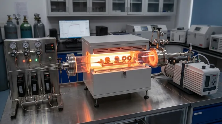
- Chemical Vapor Deposition CVD Equipment System Chamber Slide PECVD Tube Furnace with Liquid Gasifier PECVD Machine
- Customer Made Versatile CVD Tube Furnace Chemical Vapor Deposition Chamber System Equipment
- HFCVD Machine System Equipment for Drawing Die Nano-Diamond Coating
- Split Chamber CVD Tube Furnace with Vacuum Station Chemical Vapor Deposition System Equipment Machine
- Multi Heating Zones CVD Tube Furnace Machine Chemical Vapor Deposition Chamber System Equipment
People Also Ask
- What are the advantages of chemical vapor deposition? Achieve Superior Thin Films for Your Lab
- What happens during deposition chemistry? Building Thin Films from Gaseous Precursors
- What types of substrates are used in CVD to facilitate graphene films? Optimize Graphene Growth with the Right Catalyst
- What are the core advantages of PE-CVD in OLED encapsulation? Protect Sensitive Layers with Low-Temp Film Deposition
- How are carbon nanotubes grown? Master Scalable Production with Chemical Vapor Deposition


