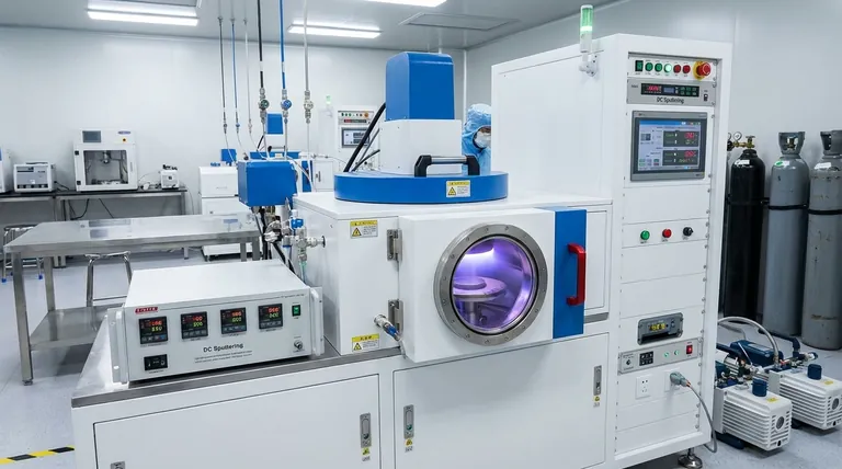
At its core, the advantage of DC sputtering lies in its simplicity and cost-effectiveness for depositing thin films of metals and other electrically conductive materials. It is a foundational Physical Vapor Deposition (PVD) technique valued for its straightforward operation, high deposition rates, and the quality of the resulting film.
DC sputtering is the go-to method for coating with conductive materials due to its low cost and high speed. However, this simplicity is also its primary limitation, as it cannot be used to deposit insulating materials.
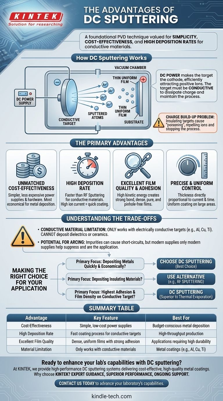
How DC Sputtering Works (And Why It Matters)
To understand the advantages, you first need to grasp the fundamental mechanism. The process itself defines both its strengths and its limitations.
The Basic Sputtering Process
Sputtering involves placing a substrate (the object to be coated) in a vacuum chamber with a "target" made of the desired coating material. An inert gas, typically argon, is introduced and ionized to create a plasma. These positive gas ions are accelerated towards the negatively charged target, striking it with enough force to eject, or "sputter," atoms of the target material. These sputtered atoms then travel through the chamber and deposit onto the substrate, forming a thin, uniform film.
The Critical Role of the DC Power Source
In DC sputtering, a direct current voltage is applied to the target, making it the cathode (negative electrode). This constant negative charge is what efficiently attracts the positive argon ions from the plasma, initiating the sputtering process. For this to work continuously, the target must be electrically conductive to dissipate the positive charge from the incoming ions and maintain the negative potential.
The "Charge Build-up" Problem with Insulators
This electrical requirement is the key to understanding DC sputtering's main limitation. If you tried to use an insulating target (like a ceramic), the positive ions would strike the surface and accumulate. This build-up of positive charge, known as "target poisoning," quickly neutralizes the negative voltage, repels other incoming ions, and shuts down the sputtering process entirely.
The Primary Advantages of DC Sputtering
When working with the right materials, DC sputtering offers a compelling set of benefits that make it a workhorse in many industries.
Unmatched Cost-Effectiveness
The power supplies and associated hardware for DC sputtering are significantly simpler and less expensive than those for other methods, like RF (Radio Frequency) sputtering. This makes it the most economical choice for many metal deposition applications.
High Deposition Rate
For conductive materials, DC sputtering is generally faster than RF sputtering. The efficient electrical circuit allows for a high ion current to the target, which directly translates into more atoms being sputtered and a quicker coating process.
Excellent Film Quality and Adhesion
Sputtered atoms have high kinetic energy when they strike the substrate. This energy promotes a strong bond, resulting in excellent film adhesion. The process also creates films that are very dense, pure, and have few pinholes compared to other techniques like thermal evaporation.
Precise and Uniform Film Control
The thickness of the deposited film is directly proportional to the target current and deposition time. This relationship makes it easy to control film thickness with high precision and repeatability. The nature of the process also allows for uniform coating over very large surface areas.
Understanding the Trade-offs
No single technique is perfect for every situation. The primary trade-off for DC sputtering's simplicity is its lack of material versatility.
The Conductive Material Limitation
As explained, DC sputtering can only be used for electrically conductive targets. This completely excludes its use for depositing dielectrics, ceramics, or other insulating compounds. For those materials, RF sputtering is the necessary alternative as it uses an alternating field that prevents charge build-up.
Potential for Arcing
While manageable, impurities or irregularities on the target surface can sometimes cause a short-circuit, or "arc." This can create defects in the film or even damage the substrate. Modern power supplies have features to suppress arcing, but it remains a consideration.
Making the Right Choice for Your Application
Selecting the correct deposition method requires matching the technique's capabilities to your project's specific goals.
- If your primary focus is depositing metals (like aluminum, copper, titanium, or platinum) quickly and economically: DC sputtering is almost always the best choice.
- If your primary focus is depositing insulating materials (like silicon dioxide or aluminum oxide): You must use an alternative method, with RF sputtering being the most common solution.
- If your primary focus is achieving the highest possible adhesion and film density on a conductive target: DC sputtering delivers superior results compared to non-sputtering techniques like thermal evaporation.
Ultimately, choosing DC sputtering is a clear decision when your application demands a high-quality, cost-effective conductive coating.
Summary Table:
| Advantage | Key Feature | Best For |
|---|---|---|
| Cost-Effectiveness | Simple, low-cost power supplies | Budget-conscious metal deposition |
| High Deposition Rate | Fast coating process for conductive targets | High-throughput production |
| Excellent Film Quality | Dense, uniform films with strong adhesion | Applications requiring high durability |
| Material Limitation | Only works with conductive materials | Metal coatings (e.g., Al, Cu, Ti) |
Ready to enhance your lab's capabilities with DC sputtering?
At KINTEK, we specialize in providing high-performance lab equipment and consumables tailored to your laboratory needs. Our DC sputtering systems are designed to deliver cost-effective, high-quality metal coatings with precision and reliability.
Why choose KINTEK?
- Expert Guidance: Our team helps you select the right equipment for your specific applications.
- Superior Performance: Achieve high deposition rates and excellent film adhesion with our reliable systems.
- Ongoing Support: We provide comprehensive support to ensure your lab operates at peak efficiency.
Contact us today to discuss how our DC sputtering solutions can benefit your research or production process. Let KINTEK be your trusted partner in advancing your laboratory's capabilities. Get in touch now!
Visual Guide
Related Products
- Spark Plasma Sintering Furnace SPS Furnace
- Multi Heating Zones CVD Tube Furnace Machine Chemical Vapor Deposition Chamber System Equipment
- Vacuum Induction Melting Spinning System Arc Melting Furnace
- Circulating Water Vacuum Pump for Laboratory and Industrial Use
People Also Ask
- What technical advantages does a Spark Plasma Sintering (SPS) furnace offer for LZP ceramics? Enhance Ionic Conductivity
- Why are Spark Plasma Sintering (SPS) furnaces or hot presses utilized in the preparation of Li3PS4 solid electrolytes?
- What is the mechanism of SPS process? A Deep Dive into Rapid, Low-Temperature Sintering
- What is the theory of spark plasma sintering? A Guide to Rapid, Low-Temperature Densification
- What is SPS sintering method? A Guide to High-Speed, High-Performance Material Fabrication


