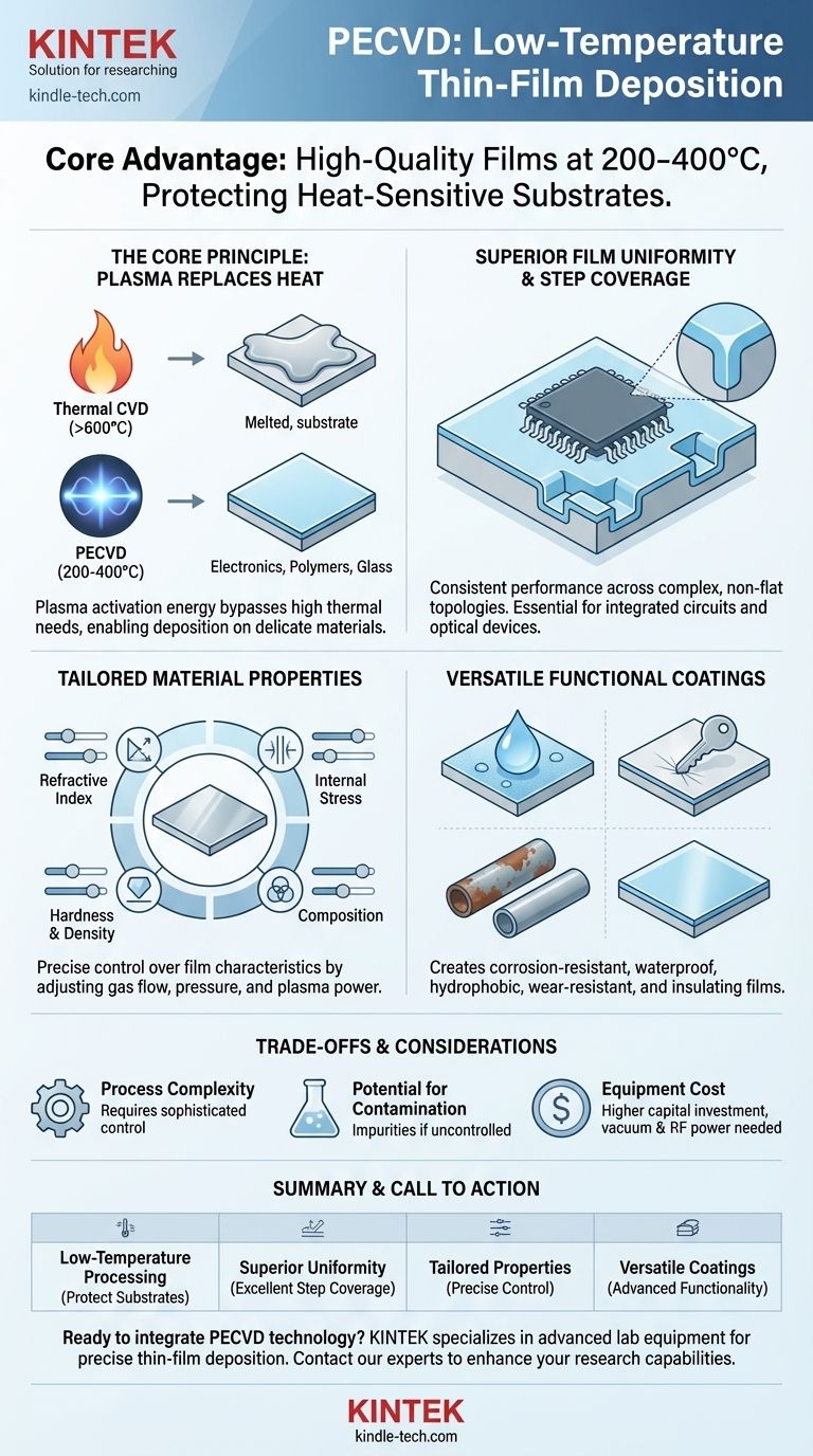
The fundamental advantage of Plasma-Enhanced Chemical Vapor Deposition (PECVD) is its ability to deposit high-quality, uniform thin films at significantly lower temperatures than traditional methods. This process bypasses the need for high thermal energy by using plasma to activate the precursor gases, enabling the creation of advanced coatings on materials that could not withstand the heat of conventional Chemical Vapor Deposition (CVD).
The core challenge in thin-film deposition is achieving a high-quality, durable film without damaging the underlying material with heat. PECVD solves this by using the energy of a plasma rather than high temperatures to drive the chemical reaction, unlocking the ability to coat heat-sensitive substrates like electronics, polymers, and glass.
The Core Principle: Bypassing High-Temperature Reactions
The most significant distinction of PECVD lies in how it initiates the film-forming chemical reaction. This unique approach is the source of its primary benefits.
How Plasma Replaces Heat
Traditional CVD requires high temperatures (often >600°C) to provide enough energy to break down precursor gases and deposit a film.
PECVD generates an energized plasma, a state of matter where gas molecules are ionized. This plasma provides the necessary activation energy, allowing the deposition reaction to occur at much lower temperatures, typically between 200°C and 400°C.
Protecting the Substrate
This low-temperature processing is critical. It allows for the deposition of high-performance films on substrates that would otherwise melt, warp, or be destroyed by conventional methods.
This capability is essential for modern manufacturing in fields like electronics and display technology, where components are often built on glass or have previously fabricated layers that are sensitive to heat.
Superior Film Quality and Control
Beyond its low-temperature operation, PECVD provides an exceptional degree of control over the final film, resulting in superior performance and consistency.
High Uniformity and Step Coverage
PECVD is renowned for producing highly uniform films with excellent step coverage. This means the coating conforms evenly over the entire surface, including complex, non-flat topologies.
This uniformity ensures consistent performance across the entire component, which is critical for applications like integrated circuits and optical devices.
Tailoring Material Properties
The process allows for precise control over the film's final characteristics. By adjusting process parameters like gas flow, pressure, and plasma power, engineers can fine-tune properties such as:
- Refractive Index: Crucial for optical coatings.
- Internal Stress: Important for preventing film cracking.
- Hardness & Density: Key for wear-resistant and protective layers.
- Composition: Allows for the creation of specific material alloys.
Creating Advanced Functional Surfaces
PECVD can create films with a wide range of desirable functional properties. These coatings provide robust protection and enhance the performance of the underlying product.
Common examples include films that are corrosion-resistant, waterproof, hydrophobic, wear-resistant, and electrically insulating or passivating.
Understanding the Trade-offs
While powerful, PECVD is not a universal solution. An objective assessment requires acknowledging its specific considerations.
Chemical and Process Complexity
The use of plasma introduces additional variables compared to thermal CVD. Managing the plasma chemistry and ensuring process stability requires sophisticated control systems and deep process knowledge.
Potential for Contamination
Precursor gases used in PECVD often contain hydrogen or other elements. If not properly controlled, these can become incorporated into the deposited film as impurities, potentially altering its desired properties.
Equipment Cost
PECVD systems, with their required vacuum chambers, gas delivery systems, and radio-frequency (RF) power sources for generating plasma, are generally more complex and carry a higher capital cost than simpler deposition techniques.
Making the Right Choice for Your Goal
Selecting PECVD is a strategic decision based on your material and performance requirements.
- If your primary focus is coating heat-sensitive substrates: PECVD is often the only viable choice for depositing high-quality films on materials like polymers, glass with existing circuitry, or complex integrated circuits.
- If your primary focus is achieving specific material properties: PECVD offers exceptional control over film density, stress, and composition, making it ideal for advanced optical coatings or precisely engineered protective layers.
- If your primary focus is uniform coverage on complex topographies: The plasma-driven process provides excellent step coverage, ensuring a consistent film thickness even over the challenging, non-flat surfaces common in microelectronics.
Ultimately, PECVD empowers engineers to create advanced materials and devices that would be impossible to fabricate using conventional high-temperature methods.
Summary Table:
| Key Advantage | Description |
|---|---|
| Low-Temperature Processing | Deposits films at 200-400°C, protecting heat-sensitive substrates like polymers and pre-fabricated electronics. |
| Superior Film Uniformity | Provides excellent step coverage and consistent thickness over complex topographies. |
| Tailored Material Properties | Allows precise control over hardness, stress, refractive index, and composition for advanced coatings. |
| Versatile Functional Coatings | Creates films that are corrosion-resistant, hydrophobic, wear-resistant, and electrically insulating. |
Ready to integrate PECVD technology into your lab? KINTEK specializes in advanced lab equipment, including PECVD systems, to help you achieve precise, low-temperature thin-film deposition for electronics, optics, and material science. Our solutions are designed to enhance your research and production capabilities with reliable, high-performance coatings. Contact our experts today to discuss your specific application needs!
Visual Guide
Related Products
- Inclined Rotary Plasma Enhanced Chemical Vapor Deposition PECVD Equipment Tube Furnace Machine
- Chemical Vapor Deposition CVD Equipment System Chamber Slide PECVD Tube Furnace with Liquid Gasifier PECVD Machine
- Inclined Rotary Plasma Enhanced Chemical Vapor Deposition PECVD Equipment Tube Furnace Machine
- RF PECVD System Radio Frequency Plasma-Enhanced Chemical Vapor Deposition RF PECVD
- Multi Heating Zones CVD Tube Furnace Machine Chemical Vapor Deposition Chamber System Equipment
People Also Ask
- What is the necessity of depositing a silicon nitride (SiNx) thin film using PECVD? Optimize QSSPC Lifetime Measurement
- Why is a PECVD system required for vertical graphene synthesis? Master Directional Control for 3D Nanostructures
- What are the advantages of plasma enhanced chemical vapor deposition? Enable Low-Temperature, High-Quality Film Deposition
- What are the benefits of plasma enhanced CVD? Achieve High-Quality, Low-Temperature Film Deposition
- What is plasma enhanced chemical vapor deposition PECVD equipment? A Guide to Low-Temperature Thin Film Deposition


