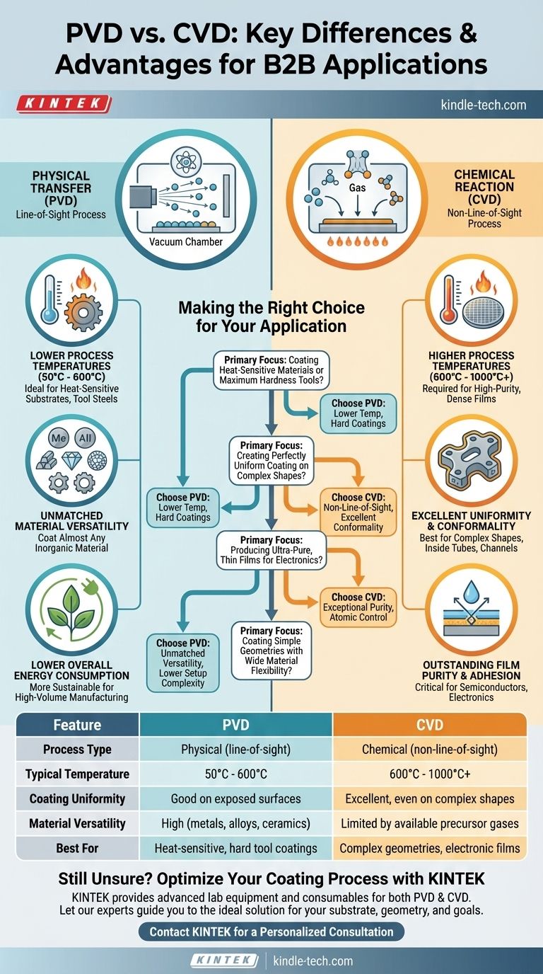
The primary advantages of Physical Vapor Deposition (PVD) over Chemical Vapor Deposition (CVD) are its lower processing temperatures and its ability to deposit a vast range of inorganic materials. PVD is a physical process that transfers material atom-by-atom, making it suitable for coating heat-sensitive substrates that would be damaged by the high temperatures of CVD. Furthermore, it consumes less energy across the entire process compared to its chemical counterpart.
Choosing between PVD and CVD is not about which is universally superior, but about aligning the process with your material, geometry, and performance goals. PVD is a physical, line-of-sight process ideal for hard coatings at lower temperatures, while CVD is a chemical process that excels at creating uniform, high-purity films on complex shapes.

The Fundamental Difference: Physics vs. Chemistry
To understand the advantages of each method, you must first grasp their core mechanisms. They are fundamentally different approaches to building a thin film.
How PVD Works: A Physical Transfer
Physical Vapor Deposition is an umbrella term for processes like sputtering and evaporation that occur in a vacuum. The concept is straightforward: a source material is physically ejected, travels through the vacuum, and condenses onto the substrate, building a coating one atom at a time.
Think of it like spray-painting on an atomic level. Particles travel in a straight line from the source (the "nozzle") to the target, which is why PVD is considered a line-of-sight process.
How CVD Works: A Chemical Reaction
Chemical Vapor Deposition introduces one or more volatile precursor gases into a reaction chamber. These gases decompose and react on the surface of a heated substrate to form the desired solid film.
This is more like baking a cake. You introduce ingredients (gases) that react under heat to form an entirely new substance (the coating). Because the gases fill the entire chamber, CVD is a non-line-of-sight process, able to coat all surfaces of a complex object evenly.
Key Advantages of PVD in Practice
The physical nature of PVD gives it distinct advantages in specific industrial and technical applications.
Lower Process Temperatures
PVD processes are performed at significantly lower temperatures than most CVD processes. Typical PVD temperatures range from 50°C to 600°C, while CVD often requires temperatures of 600°C to over 1000°C.
This is PVD's most critical advantage. It allows for the coating of hardened tool steels, plastics, and other materials that cannot withstand the intense heat of CVD without being damaged, softened, or distorted.
Unmatched Material Versatility
Because PVD physically transports material, it can be used to deposit almost any inorganic material, including pure metals, alloys, and a wide variety of ceramic compounds. If a material can be made into a solid target, it can likely be deposited via PVD.
CVD, by contrast, is limited by the availability of suitable precursor gases that can chemically react to form the desired film at a reasonable temperature.
Lower Overall Energy Consumption
Multiple sustainability assessments have demonstrated that when considering all process steps, PVD has a lower overall energy footprint than CVD. This is a significant factor for high-volume manufacturing where operational costs are a primary concern.
Understanding the Trade-offs: When CVD Excels
No technology is without limitations. PVD's advantages come with trade-offs that make CVD the better choice for other applications.
The "Line-of-Sight" Limitation
PVD's greatest weakness is its line-of-sight nature. It cannot effectively coat the inside of long tubes, complex internal channels, or the backside of an object without complex and expensive part rotation mechanisms. The coating will be thickest on surfaces directly facing the source and thinnest or non-existent in shadowed areas.
The Strength of CVD: Uniformity on Complex Shapes
This is where CVD shines. Because the precursor gases flow around and inside the part, CVD provides an exceptionally uniform and conformal coating, even on parts with intricate geometries. The thickness of the coating is consistent across all surfaces.
Film Purity and Adhesion
While PVD adhesion is good, the chemical bond formed between the substrate and the film during a high-temperature CVD process can result in outstanding adhesion. CVD is also known for its ability to produce films of extremely high purity, which is critical for applications in semiconductors and electronics.
Making the Right Choice for Your Application
The decision to use PVD or CVD should be driven entirely by the requirements of your project.
- If your primary focus is coating heat-sensitive materials or achieving maximum hardness on tools: Choose PVD for its lower process temperatures and ability to deposit exceptionally hard ceramic coatings.
- If your primary focus is creating a perfectly uniform coating on a complex, non-flat part: Choose CVD for its non-line-of-sight deposition and excellent conformality.
- If your primary focus is producing ultra-pure, thin films for electronics: Choose CVD, as its chemical reaction process allows for exceptional purity and atomic-level control.
- If your primary focus is coating simple geometries with a wide variety of metals or alloys: Lean towards PVD for its unmatched material flexibility and lower setup complexity compared to developing new CVD chemistries.
By understanding the core mechanism of each process, you can confidently select the technology that meets your specific engineering goals.
Summary Table:
| Feature | PVD (Physical Vapor Deposition) | CVD (Chemical Vapor Deposition) |
|---|---|---|
| Process Type | Physical (line-of-sight) | Chemical (non-line-of-sight) |
| Typical Temperature | 50°C - 600°C | 600°C - 1000°C+ |
| Coating Uniformity | Good on directly exposed surfaces | Excellent, even on complex shapes |
| Material Versatility | High (metals, alloys, ceramics) | Limited by available precursor gases |
| Best For | Heat-sensitive substrates, hard tool coatings | Complex geometries, ultra-pure electronic films |
Still unsure which coating process is right for your application?
The choice between PVD and CVD is critical for achieving your desired material performance and coating quality. KINTEK specializes in providing advanced lab equipment and consumables for both processes, helping you optimize your R&D and production.
Let our experts guide you to the ideal solution for your specific substrate, geometry, and performance goals.
Contact KINTEK today for a personalized consultation and discover how our expertise can enhance your laboratory's capabilities.
Visual Guide
Related Products
- RF PECVD System Radio Frequency Plasma-Enhanced Chemical Vapor Deposition RF PECVD
- Split Chamber CVD Tube Furnace with Vacuum Station Chemical Vapor Deposition System Equipment Machine
- Chemical Vapor Deposition CVD Equipment System Chamber Slide PECVD Tube Furnace with Liquid Gasifier PECVD Machine
- VHP Sterilization Equipment Hydrogen Peroxide H2O2 Space Sterilizer
- 1400℃ Controlled Atmosphere Furnace with Nitrogen and Inert Atmosphere
People Also Ask
- What is an example of PECVD? RF-PECVD for High-Quality Thin Film Deposition
- What are the benefits of PECVD? Achieve Superior Low-Temperature Thin Film Deposition
- How does RF power create plasma? Achieve Stable, High-Density Plasma for Your Applications
- What is the principle of plasma enhanced chemical vapor deposition? Achieve Low-Temperature Thin Film Deposition
- What are the advantages of PECVD? Enable Low-Temperature, High-Quality Thin-Film Deposition