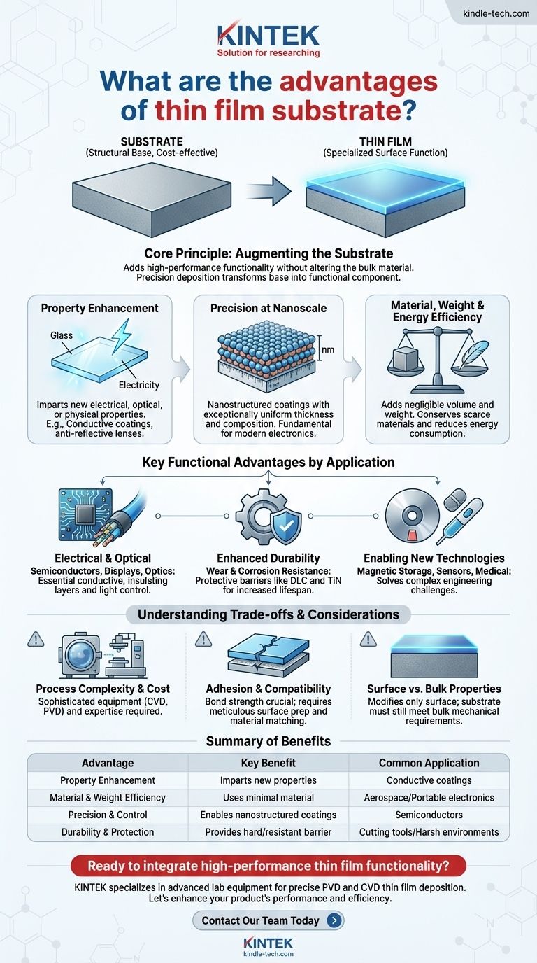
In practice, the advantages of using thin films on a substrate are about adding high-performance functionality without altering the bulk material. This technology allows engineers to impart entirely new electrical, optical, or physical properties onto a surface, enabling the creation of smaller, more efficient, and more durable products while conserving expensive or rare materials.
The core advantage of thin film technology is not in the substrate itself, but in the ability to precisely deposit a microscopic layer of a different material onto it. This transforms a simple, often inexpensive, structural base into a highly functional component with specialized surface properties.
The Core Principle: Augmenting the Substrate
A thin film and its substrate work as a team. The substrate provides the mechanical structure, form factor, and a cost-effective foundation. The thin film provides the specialized, high-value surface function that the substrate material lacks.
Adding What Isn't There
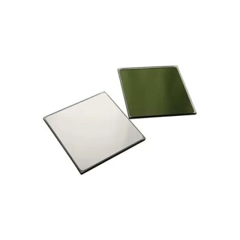
A primary advantage is the ability to bestow new properties on a material. A simple piece of glass or plastic can be transformed into a conductive surface, an electrical insulator, or an anti-reflective lens.
This is achieved by depositing a film with the desired characteristic—such as a metal for conductivity or a ceramic for insulation—onto the base material.
Precision at the Nanoscale
Thin film deposition processes operate at the atomic and molecular levels, allowing for the creation of nanostructured coatings with exceptionally uniform thickness and composition.
This level of control is fundamental to modern electronics, where layers just a few atoms thick can define the function of a transistor or memory cell.
Efficiency in Material, Weight, and Energy
Because the functional layer is incredibly thin, it adds negligible volume or weight to the final product. This is critical for aerospace, portable electronics, and medical implants.
This approach also conserves scarce or expensive materials, as only a microscopic amount is needed. Furthermore, many modern deposition processes are designed to reduce energy consumption and effluent output compared to bulk material processing.
Key Functional Advantages by Application
The specific benefits of thin films become clearest when viewed through the lens of their applications in different industries.
Electrical and Optical Manipulation
In semiconductors and displays, thin films are not an advantage—they are a necessity. They serve as the conductive, insulating, and semiconducting layers that form integrated circuits.
For optics, thin films are used to create coatings that offer scratch resistance, control reflection and transmission of light, or filter specific wavelengths.
Enhanced Durability and Resistance
Thin films can act as a protective barrier. Hard coatings like Diamond-Like Carbon (DLC) or Titanium Nitride (TiN) are applied to cutting tools and wear components to dramatically increase their lifespan and performance.
These films also provide excellent corrosion resistance, protecting the underlying substrate from harsh environmental conditions.
Enabling New Technologies
Many modern engineering challenges are solved by thin films. This technology is essential for creating magnetic storage media, specialized sensors, and biocompatible coatings for medical devices.
It allows for the development of entirely new products and solutions that would be physically or economically impossible to create using bulk materials alone.
Understanding the Trade-offs and Considerations
While powerful, thin film technology is not a universal solution. Its application requires careful consideration of its complexities and limitations.
Process Complexity and Cost
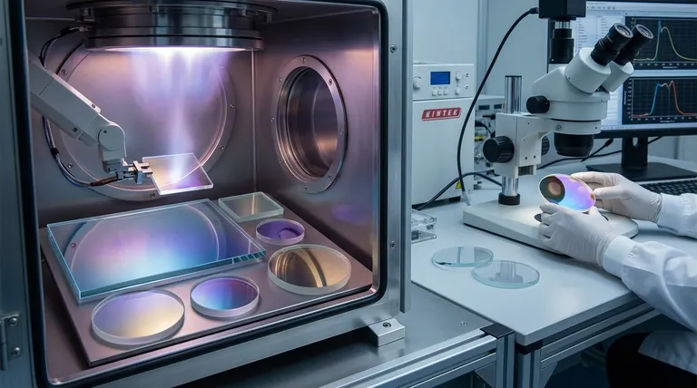
Depositing a high-quality thin film requires sophisticated equipment and a highly controlled environment, such as a vacuum.
Processes like Chemical Vapor Deposition (CVD) and Physical Vapor Deposition (PVD) involve significant capital investment and deep process expertise, making them more complex than simple mechanical coating methods.
Adhesion and Substrate Compatibility
A thin film is only as effective as its bond to the substrate. Poor adhesion can lead to delamination and device failure.
Success depends heavily on selecting compatible materials, meticulous surface preparation of the substrate, and fine-tuning deposition process parameters.
Surface vs. Bulk Properties
It is crucial to remember that a thin film only modifies the surface of a component. It does not change the substrate's bulk properties, such as its overall mechanical strength, thermal conductivity, or density.
Engineers must design the component so the substrate meets all structural requirements, while the film handles the required surface function.
Making the Right Choice for Your Goal
Selecting the right material strategy depends entirely on your primary objective.
- If your primary focus is miniaturization or performance density: Thin film deposition is the fundamental technology for adding function without adding significant mass or volume.
- If your primary focus is surface durability and protection: Use thin film coatings to give a cost-effective substrate superior wear resistance, hardness, or corrosion protection.
- If your primary focus is advanced electronics or optics: Thin films are an essential, non-negotiable part of manufacturing semiconductors, displays, and high-performance optical components.
Ultimately, thin film technology empowers you to use the right material for the right job—structure from the substrate, and function from the film.
Summary Table:
| Advantage | Key Benefit | Common Application |
|---|---|---|
| Property Enhancement | Imparts new electrical, optical, or physical properties to a surface. | Conductive coatings on glass, anti-reflective lenses. |
| Material & Weight Efficiency | Uses minimal material, adding negligible weight and conserving resources. | Aerospace components, portable electronics, medical implants. |
| Precision & Control | Enables nanostructured coatings with uniform thickness at the atomic level. | Semiconductors, integrated circuits, memory cells. |
| Durability & Protection | Provides a hard, wear-resistant, or corrosion-resistant barrier. | Cutting tools (DLC, TiN coatings), components in harsh environments. |
Ready to integrate high-performance thin film functionality into your products?
At KINTEK, we specialize in providing the advanced lab equipment and consumables necessary for precise thin film deposition processes like PVD and CVD. Whether you are developing smaller electronics, more durable components, or innovative optical systems, our solutions help you achieve the exact surface properties your project demands.
Let's discuss how our expertise can enhance your product's performance and efficiency. Contact our team today for a personalized consultation!
Visual Guide
Related Products
- Electron Beam Evaporation Coating Oxygen-Free Copper Crucible and Evaporation Boat
- Optical Window Glass Substrate Wafer Single Double Sided Coated K9 Quartz Sheet
- Optical Window Glass Substrate Wafer Quartz Plate JGS1 JGS2 JGS3
- Infrared Transmission Coating Sapphire Sheet Substrate Window
- MgF2 Magnesium Fluoride Crystal Substrate Window for Optical Applications
People Also Ask
- How is an electron beam evaporator cooled during deposition? Essential Thermal Management for Stable Processes
- What is the current of e-beam evaporation? A Guide to High-Purity Thin Film Deposition
- What is the deposition rate of e-beam evaporation? Control Thin Film Quality and Speed
- What is the container that holds the metal source material called in e-beam evaporation? Ensure Purity and Quality in Your Thin-Film Deposition
- What are the applications of e-beam evaporation? Achieve High-Purity Coatings for Optics & Electronics