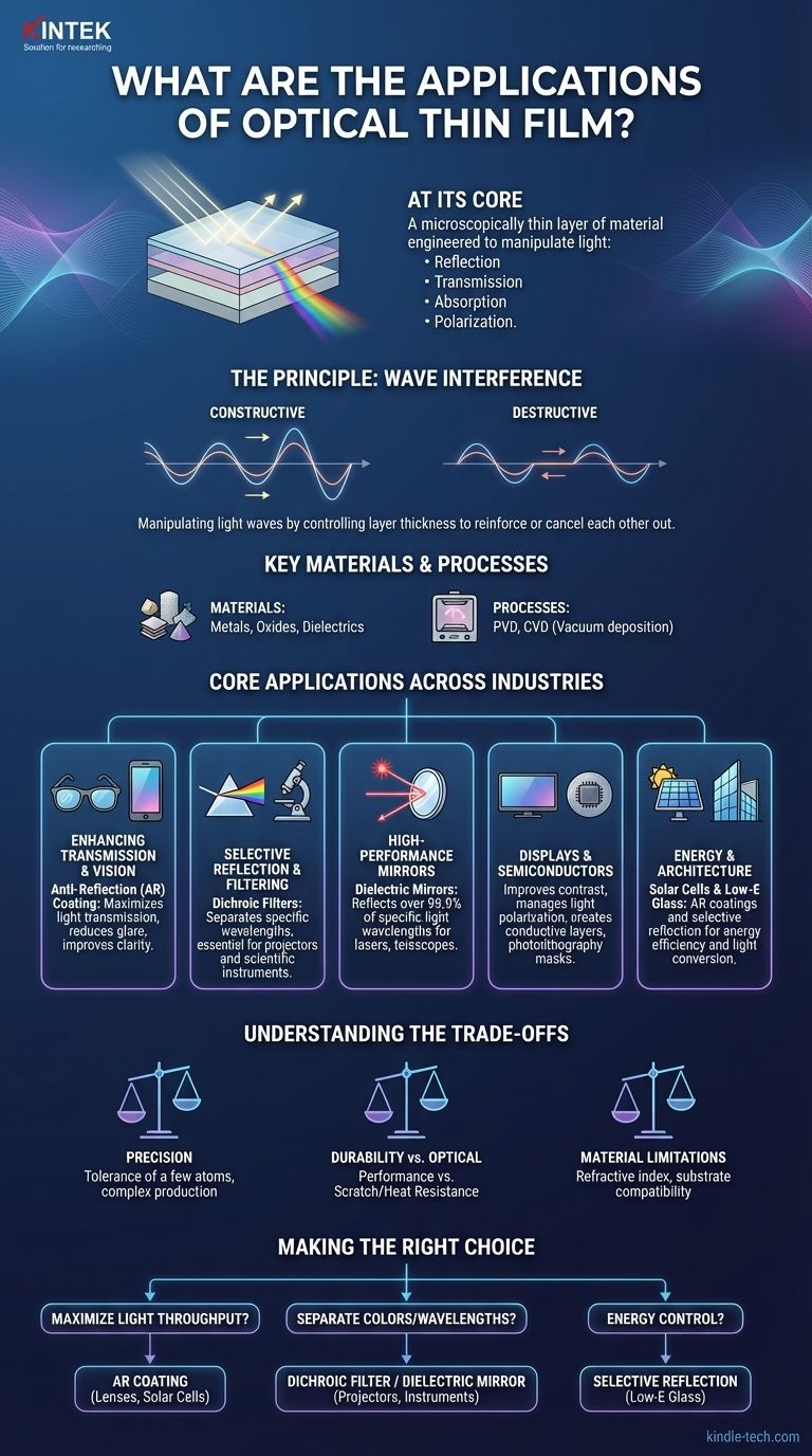
At its core, an optical thin film is a microscopically thin layer of material engineered to manipulate light. Its applications are widespread, ranging from the anti-reflection coatings on your eyeglasses and camera lenses to the high-precision filters used in scientific instruments, solar cells, and modern display technologies.
The fundamental purpose of an optical thin film is not merely to cover a surface, but to precisely control how light is reflected, transmitted, absorbed, or polarized by leveraging the principles of wave interference at a nanometer scale.

The Principle Behind the Application
Before listing applications, it's crucial to understand how these films work. Their function is not based on the bulk properties of the material but on the precise thickness of the layers.
The Power of Interference
Optical thin films are often composed of multiple layers, each with a thickness comparable to the wavelength of light. As light waves pass through these layers, they reflect off each interface.
These reflected waves can either reinforce each other (constructive interference) or cancel each other out (destructive interference). By carefully designing the thickness and material of each layer, we can control which wavelengths of light are reflected and which are transmitted.
Key Materials and Processes
These precise layers are created from materials like metals, oxides, and dielectrics (non-conductive ceramics).
The films are deposited using highly controlled vacuum processes like Physical Vapor Deposition (PVD), which involves sputtering or evaporating material onto a surface, and Chemical Vapor Deposition (CVD), which uses gas precursors to form the coating.
Core Applications Across Industries
The ability to finely tune the properties of light gives optical thin films an incredibly diverse range of uses.
Enhancing Transmission and Vision
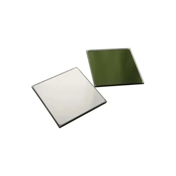
The most common application is anti-reflection (AR) coating. By using destructive interference to eliminate reflections, these films maximize light transmission. You find them on eyeglasses, camera lenses, solar panels, and the screens of smartphones and laptops to reduce glare and improve clarity.
Selective Reflection and Filtering
Conversely, films can be designed to reflect specific wavelengths while transmitting others. These are known as dichroic filters. They are critical in digital projectors to separate red, green, and blue light, and in scientific instruments like fluorescence microscopes to isolate specific light frequencies.
High-Performance Mirrors
While a standard mirror uses a simple layer of metal, high-performance dielectric mirrors use dozens of alternating thin film layers. This allows them to reflect over 99.9% of light within a specific wavelength range, making them essential for lasers, telescopes, and other precision optical systems.
Displays and Semiconductors
In flat-panel displays, thin films are used to improve contrast, manage light polarization, and create transparent conductive layers for touch screens. In semiconductor manufacturing, they are used as critical masks and anti-reflective layers during the photolithography process, which etches circuits onto silicon wafers.
Energy and Architecture
In solar cells, thin films serve a dual purpose: as AR coatings to ensure more light enters the cell and as functional layers that help convert that light into electricity. In modern architecture, low-emissivity (Low-E) glass is coated with thin films that reflect infrared radiation (heat) while allowing visible light to pass, dramatically improving energy efficiency.
Understanding the Trade-offs
While powerful, the application of optical thin films involves significant engineering challenges.
Precision is Non-Negotiable
The performance of an optical film is entirely dependent on its thickness, often with a tolerance of just a few atoms. Any deviation during the manufacturing process can render the coating useless, making production complex and expensive.
Durability vs. Optical Performance
The materials that produce the best optical effects are not always the most durable. There is a constant trade-off between creating a coating that can withstand scratches, heat, and environmental exposure and one that perfectly meets its optical specifications.
Material and Substrate Limitations
The choice of coating material is limited by its refractive index and compatibility with both the substrate (the glass or plastic it's applied to) and the deposition process. Not all materials can be effectively layered onto all substrates.
Making the Right Choice for Your Goal
The specific design of an optical thin film is dictated entirely by its intended function.
- If your primary focus is maximizing light throughput: You need an anti-reflection (AR) coating designed to cancel out reflections for your target wavelengths, as seen in lenses and solar cells.
- If your primary focus is separating colors or wavelengths: You need a multi-layer dichroic filter or dielectric mirror designed for selective reflection and transmission, essential for projectors and scientific instruments.
- If your primary focus is energy control: You need a coating that selectively reflects specific parts of the spectrum, like the infrared-blocking films used in architectural glass.
Ultimately, optical thin films are a foundational, yet often invisible, technology that shapes our modern world by precisely directing the flow of light.
Summary Table:
| Application Area | Key Function of Thin Film | Common Examples |
|---|---|---|
| Consumer Optics | Anti-Reflection (AR) | Eyeglasses, camera lenses, smartphone screens |
| Scientific Instruments | Wavelength Filtering | Fluorescence microscopes, lasers, telescopes |
| Displays & Electronics | Light Polarization & Conduction | Flat-panel displays, touch screens, semiconductor lithography |
| Energy & Architecture | Selective Reflection/Transmission | Solar cells, Low-E energy-efficient glass |
Ready to integrate precision optical coatings into your project? KINTEK specializes in high-performance lab equipment and consumables, including advanced deposition systems for creating optical thin films. Whether you're developing next-generation displays, sensitive scientific instruments, or efficient solar technology, our solutions ensure the accuracy and durability your applications demand. Contact our experts today to discuss how we can support your laboratory's specific needs and help you achieve superior optical performance.
Visual Guide
Related Products
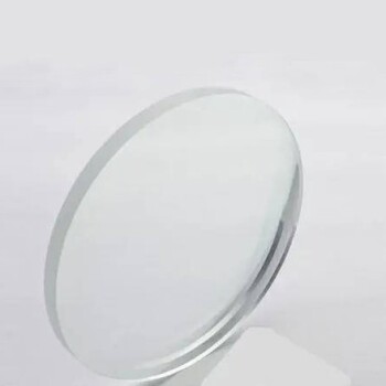
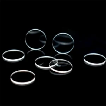
- Infrared Transmission Coating Sapphire Sheet Substrate Window
- Optical Ultra-Clear Glass Sheet for Laboratory K9 B270 BK7
- High Temperature Resistant Optical Quartz Glass Sheet
- MgF2 Magnesium Fluoride Crystal Substrate Window for Optical Applications
- Optical Window Glass Substrate Wafer Single Double Sided Coated K9 Quartz Sheet
People Also Ask
- Is Sputter Tint good? Premium Heat Rejection & Long-Term Durability Explained
- What is organic thin film? A Guide to Engineered Molecular Layers for Advanced Tech
- How can we create a reducing environment? Master the Methods for Precise Chemical Control
- What are the applications of optical coating? Unlock Advanced Light Control for Your Industry
- How do cooling jackets or heat exchangers contribute to the stability of glycerol conversion? Master Thermal Management