From the microchip in your phone to the drill bit in a factory, Physical Vapor Deposition (PVD) is a critical coating technology used across a vast range of industries. It is applied to everything from medical implants and cutting tools to jewelry and optical lenses. The core function of PVD is to deposit a very thin, high-performance layer of material onto a surface to dramatically enhance its properties, such as durability, corrosion resistance, and appearance.
The true value of PVD lies not just in its wide range of applications, but in its unique ability to solve fundamental material science challenges. It allows engineers to apply incredibly pure, hard, and thin coatings to surfaces that cannot be treated by other methods, fundamentally changing the performance and lifespan of a product.
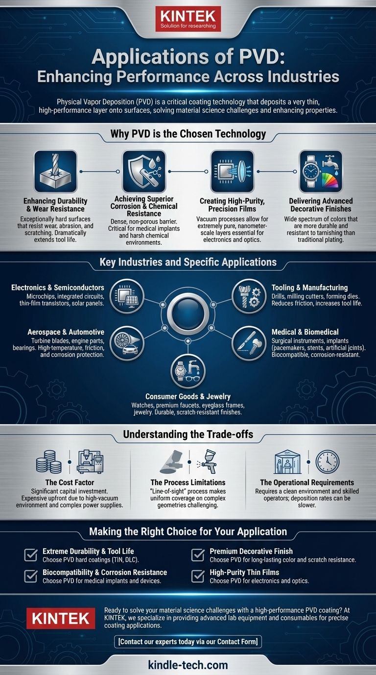
Why PVD is the Chosen Technology
PVD is not simply a decorative finish; it is an advanced engineering process that imparts specific, high-value properties to a substrate. Industries choose it when performance and reliability are non-negotiable.
Enhancing Durability and Wear Resistance
The most common application of PVD is to create an exceptionally hard surface that resists wear, abrasion, and scratching.
These coatings, often harder than steel, dramatically extend the functional life of tools and components, reducing downtime and replacement costs in demanding industrial environments.
Achieving Superior Corrosion and Chemical Resistance
PVD creates a dense, non-porous film that acts as an impenetrable barrier between the component and its environment.
This is critical for medical implants, which must be biocompatible and resist corrosion from bodily fluids, as well as for parts used in harsh chemical or marine settings.
Creating High-Purity, Precision Films
PVD processes occur in a vacuum, which allows for the deposition of extremely pure and clean material layers.
This is essential for the electronics industry, where PVD is used to create the nanometer-scale films in microchips and semiconductors. It is also used for optical lenses to create precise anti-reflective or reflective coatings.
Delivering Advanced Decorative Finishes
While highly functional, PVD also offers superior decorative options. It can produce a wide spectrum of colors that are far more durable and resistant to tarnishing and fading than traditional methods like electroplating.
This makes it a preferred choice for high-end consumer goods like watches, faucets, and premium hardware.
Key Industries and Specific Applications
The properties imparted by PVD translate directly into tangible benefits across several key sectors.
Electronics and Semiconductors
PVD methods like sputtering are fundamental to modern electronics. They are used to deposit the conductive and insulating layers in integrated circuits, thin-film transistors for displays, and conductive coatings for solar panels.
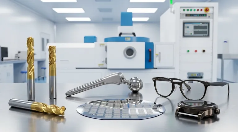
Tooling and Manufacturing
This is a classic application for PVD. Hard coatings like Titanium Nitride (TiN) and Diamond-Like Carbon (DLC) are applied to drills, milling cutters, and forming dies. This reduces friction, prevents material buildup, and can increase tool life by a factor of ten or more.
Medical and Biomedical
Because the coatings are inert and biocompatible, PVD is essential for medical devices. It is used on surgical instruments for hardness and sterility, and on implants like pacemakers, stents, and artificial joints to prevent rejection and corrosion.
Aerospace and Automotive
In aerospace and automotive, every gram matters. PVD provides thin, lightweight coatings that protect critical components from high temperatures, friction, and corrosion without adding significant weight. This is used on turbine blades, engine parts, and bearings.
Consumer Goods and Jewelry
PVD provides the durable, brilliant finishes on high-end watches, premium faucets, eyeglass frames, and jewelry. It ensures the product maintains its "day one" appearance by resisting scratches and discoloration from daily use.
Understanding the Trade-offs
While powerful, PVD is not a universal solution. An objective assessment requires understanding its limitations.
The Cost Factor
PVD equipment represents a significant capital investment. The process requires a high-vacuum environment, complex power supplies, and often a cooling system, making it more expensive upfront than some traditional coating methods.
The Process Limitations
Most PVD processes are "line-of-sight," meaning the coating source must have a direct path to the surface being coated. This can make it challenging to achieve uniform coverage on parts with complex, intricate geometries.
The Operational Requirements
PVD is a sophisticated process that requires a clean environment and skilled operators. The deposition rates can also be slower than other methods, which can limit throughput for high-volume, low-cost items.
Making the Right Choice for Your Application
Selecting the right coating technology depends entirely on your primary goal.
- If your primary focus is extreme durability and tool life: PVD hard coatings like TiN or DLC are the industry standard for cutting tools and high-wear components.
- If your primary focus is biocompatibility and corrosion resistance: PVD is a leading choice for medical implants and devices due to its inert, pure, and robust barrier properties.
- If your primary focus is a premium, long-lasting decorative finish: PVD offers a wide range of colors with superior resistance to scratches and tarnishing compared to traditional plating.
- If your primary focus is high-purity thin films for electronics or optics: PVD methods are essential for creating the precise, nanometer-scale layers required in semiconductors and advanced lenses.
Understanding these core capabilities allows you to specify PVD not just as a coating, but as a strategic solution to a fundamental engineering challenge.
Summary Table:
| Industry | Key PVD Applications | Primary Benefits |
|---|---|---|
| Electronics & Semiconductors | Microchips, Solar Panels | High-purity, conductive films |
| Tooling & Manufacturing | Drills, Milling Cutters | Extreme wear resistance, longer tool life |
| Medical & Biomedical | Surgical Instruments, Implants | Biocompatibility, corrosion resistance |
| Aerospace & Automotive | Turbine Blades, Engine Parts | High-temperature resistance, lightweight |
| Consumer Goods & Jewelry | Watches, Faucets, Eyeglasses | Durable, scratch-resistant decorative finishes |
Ready to solve your material science challenges with a high-performance PVD coating?
At KINTEK, we specialize in providing advanced lab equipment and consumables for precise coating applications. Whether you are developing new semiconductor components, manufacturing longer-lasting tools, or creating durable medical devices, our solutions can help you achieve superior surface properties.
Contact our experts today via our Contact Form to discuss how we can support your specific laboratory and production needs.
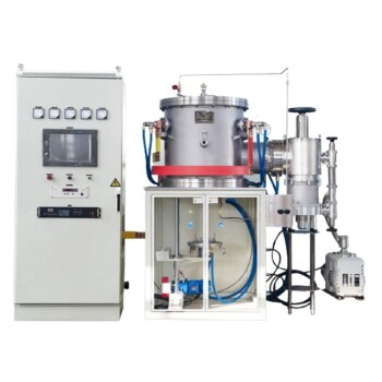
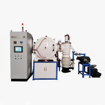
Visual Guide
Related Products
- RF PECVD System Radio Frequency Plasma-Enhanced Chemical Vapor Deposition RF PECVD
- Chemical Vapor Deposition CVD Equipment System Chamber Slide PECVD Tube Furnace with Liquid Gasifier PECVD Machine
- Split Chamber CVD Tube Furnace with Vacuum Station Chemical Vapor Deposition System Equipment Machine
- Molybdenum Tungsten Tantalum Special Shape Evaporation Boat
- VHP Sterilization Equipment Hydrogen Peroxide H2O2 Space Sterilizer
People Also Ask
- What are the benefits of PECVD? Achieve Superior Low-Temperature Thin Film Deposition
- Why does PECVD commonly use RF power input? For Precise Low-Temperature Thin Film Deposition
- What is the principle of plasma enhanced chemical vapor deposition? Achieve Low-Temperature Thin Film Deposition
- What are the advantages of PECVD? Enable Low-Temperature, High-Quality Thin-Film Deposition
- What is an example of PECVD? RF-PECVD for High-Quality Thin Film Deposition