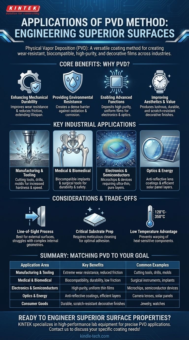
In short, Physical Vapor Deposition (PVD) is a coating method used across a vast range of industries, from manufacturing and medicine to electronics and consumer goods. Its applications include creating wear-resistant cutting tools, biocompatible medical implants, high-purity semiconductor layers, and decorative finishes for jewelry.
PVD is not just a simple coating process; it is a strategic engineering tool. It allows you to impart new, high-performance properties onto the surface of a material—such as extreme hardness or chemical resistance—without altering the core structure of the underlying component.

Why PVD is the Chosen Method: Core Benefits
The versatility of PVD comes from its ability to fundamentally enhance a material's surface. These enhancements solve specific engineering and design challenges.
Enhancing Mechanical Durability
PVD coatings create an incredibly hard, thin film that dramatically improves wear resistance and reduces friction. This is critical for components that experience significant mechanical stress.
This enhancement extends the functional lifespan of parts, allowing them to perform more efficiently and for longer periods.
Providing Environmental and Chemical Resistance
Many applications require components to operate in harsh environments. PVD provides a dense, non-porous barrier against the substrate.
This layer improves oxidation and corrosion resistance, protecting the underlying material and preventing premature failure.
Enabling Advanced Electronic and Optical Functions
PVD is capable of depositing extremely pure, thin, and uniform films. This level of precision is essential in high-technology fields.
It is used to create conductive pathways in microchips, anti-reflective coatings on optical lenses, and efficient layers in solar panels where purity and consistency directly impact performance.
Improving Aesthetics and Value
Beyond functional benefits, PVD is used to enhance the appearance of consumer products. It can produce a lustrous, durable finish or change a metal's color.
This application is common in the jewelry and watch industries, where it provides a finish that is both beautiful and highly resistant to scratches and tarnishing.
Key Industrial Applications
The theoretical benefits of PVD translate into concrete, real-world applications across multiple sectors.
Manufacturing and Tooling
The most common application is on cutting tools, drills, and molds. A PVD coating can increase the tool's hardness and reduce friction, allowing for faster cutting speeds, longer life, and a better finish on the machined part.
Medical and Biomedical
PVD coatings are crucial for medical implants (like hip or knee joints) and surgical instruments. The coatings are biocompatible, highly durable, and provide a low-friction surface that minimizes wear inside the body.
Electronics and Semiconductors
In microelectronics, PVD is essential for fabricating semiconductor devices and microchips. The process deposits the ultra-thin, high-purity layers of conductive and insulating materials that form integrated circuits.
Optics and Energy
PVD is used to apply anti-reflective coatings on eyeglass lenses and camera optics, improving clarity and performance. In the energy sector, it is used to create the functional layers within solar panels.
Understanding the Trade-offs and Considerations
While powerful, PVD is a precise process with specific requirements that make it suitable for some applications but not others.
It Is a Line-of-Sight Process
PVD works by transferring coating material in a straight line from the source to the substrate. This means it is exceptionally good at coating external surfaces but struggles with complex internal geometries or hidden areas.
Substrate Preparation is Critical
The exceptional performance of a PVD coating depends on its adhesion to the substrate. This requires the part to be meticulously cleaned before entering the coating chamber, as any surface contamination will compromise the bond.
Low Temperature is a Major Advantage
PVD is a low-temperature process, typically operating between 120°C and 350°C. This is a significant benefit, as it allows for the coating of precision-engineered or heat-sensitive components without causing them to warp, anneal, or lose their dimensional accuracy.
Matching the PVD Application to Your Goal
Your choice to use PVD should be driven by the specific surface property you need to achieve.
- If your primary focus is extending tool life and performance: PVD is the industry standard for creating hard, low-friction coatings on cutting tools, dies, and wear components.
- If your primary focus is high-purity functional films: PVD provides the precision and cleanliness required for semiconductors, optical lenses, and solar cells.
- If your primary focus is biocompatibility and durability: PVD is a proven method for coating medical implants and surgical tools to ensure safety and longevity.
- If your primary focus is a premium aesthetic finish: PVD offers a durable, decorative, and scratch-resistant solution for watches, jewelry, and other consumer goods.
Ultimately, PVD empowers you to engineer the surface of a component to meet demands its base material cannot.
Summary Table:
| Application Area | Key Benefits of PVD | Common Examples |
|---|---|---|
| Manufacturing & Tooling | Extreme wear resistance, reduced friction | Cutting tools, drills, molds |
| Medical & Biomedical | Biocompatibility, durability, low friction | Surgical instruments, implants (hips, knees) |
| Electronics & Semiconductors | High-purity, uniform thin films | Microchips, semiconductor devices |
| Optics & Energy | Anti-reflective coatings, efficient layers | Camera lenses, solar panels |
| Consumer Goods | Durable, scratch-resistant decorative finishes | Jewelry, watches |
Ready to engineer superior surface properties with PVD? KINTEK specializes in high-performance lab equipment and consumables for precise PVD applications. Whether you're in manufacturing, medical, or electronics, our solutions help you achieve enhanced durability, purity, and aesthetics. Contact us today to discuss how we can support your specific coating needs!
Visual Guide
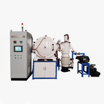
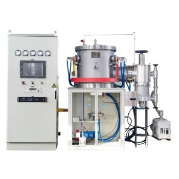
Related Products
- RF PECVD System Radio Frequency Plasma-Enhanced Chemical Vapor Deposition RF PECVD
- Chemical Vapor Deposition CVD Equipment System Chamber Slide PECVD Tube Furnace with Liquid Gasifier PECVD Machine
- Split Chamber CVD Tube Furnace with Vacuum Station Chemical Vapor Deposition System Equipment Machine
- Aluminized Ceramic Evaporation Boat for Thin Film Deposition
- 1400℃ Controlled Atmosphere Furnace with Nitrogen and Inert Atmosphere
People Also Ask
- What are the advantages of PECVD? Enable Low-Temperature, High-Quality Thin-Film Deposition
- What is plasma activated chemical vapour deposition method? A Low-Temperature Solution for Advanced Coatings
- What are the applications of PECVD? Essential for Semiconductors, MEMS, and Solar Cells
- What is an example of PECVD? RF-PECVD for High-Quality Thin Film Deposition
- Why does PECVD commonly use RF power input? For Precise Low-Temperature Thin Film Deposition