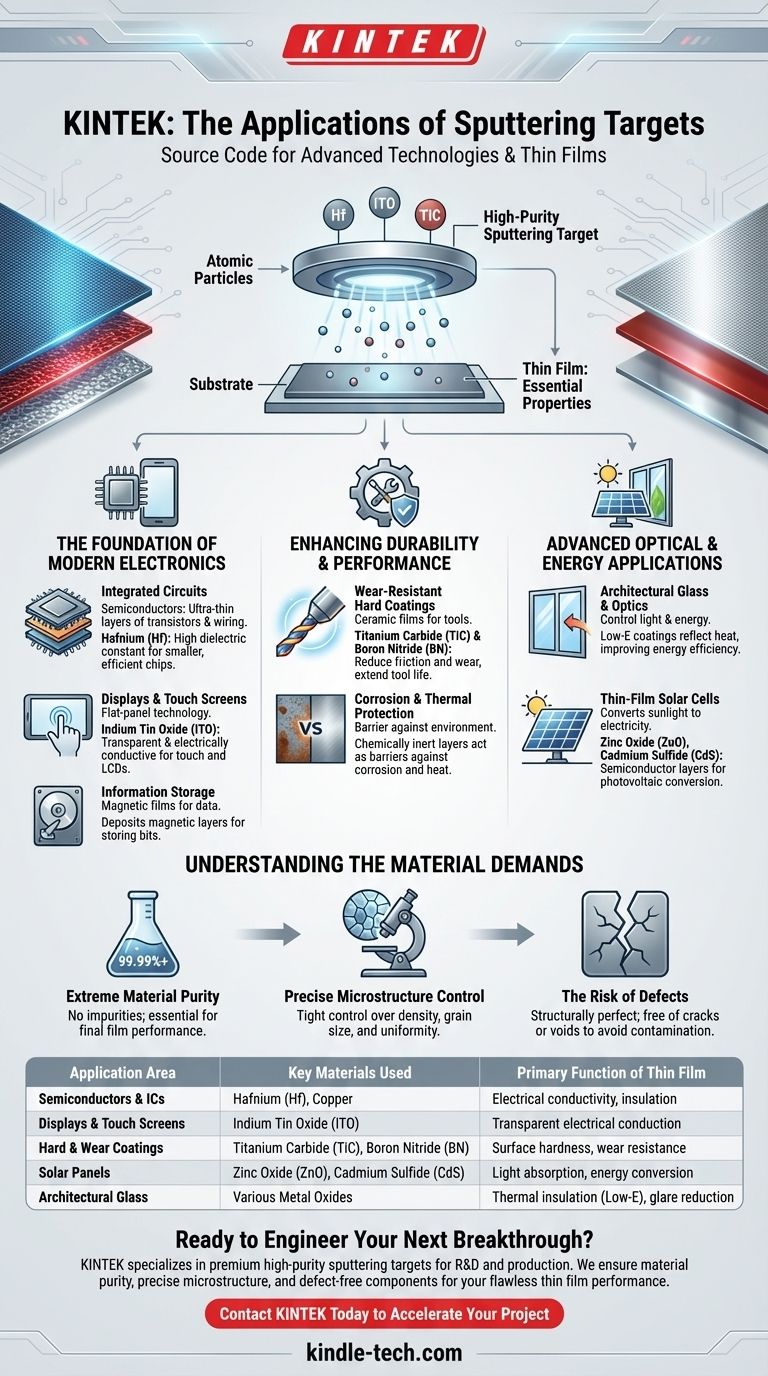
In short, sputtering targets are the high-purity source materials used to create the microscopic thin films that define modern technology. These films are deposited onto surfaces to give them essential properties, making sputtering a cornerstone process in industries ranging from electronics and information storage to solar energy and protective coatings for tools.
The core application of a sputtering target is not the material itself, but the high-performance thin film it produces. This process allows engineers to deposit precise layers of material—sometimes only a few atoms thick—to add critical functions like electrical conductivity, insulation, wear resistance, or optical properties to a product.
The Foundation of Modern Electronics
Sputtering is an indispensable process for fabricating the components that power our digital world. The precision of thin-film deposition is what enables the miniaturization and high performance of electronic devices.
Integrated Circuits (Semiconductors)
Sputtering is used to deposit the ultra-thin layers of conductive and insulating materials that form the transistors and wiring within a microchip.
For example, hafnium (Hf) targets are used to create films with a high dielectric constant, a critical property that allows for smaller, more efficient, and more powerful semiconductors.
Displays and Touch Screens
Virtually every flat-panel display, from your smartphone to your television, relies on sputtered films.
Indium Tin Oxide (ITO) targets are a primary example. They are used to create a film that is both optically transparent and electrically conductive, the essential combination that makes touch screens and LCDs possible.
Information Storage
The ability to store vast amounts of data on hard drives and other media depends on sputtered magnetic films. Sputtering deposits the complex layers of materials that can be magnetized to represent the bits and bytes of digital information.
Enhancing Durability and Performance
Beyond electronics, sputtering is widely used to apply protective coatings that dramatically extend the service life and performance of tools and components. These functional coatings are engineered for specific environmental challenges.
Wear-Resistant Hard Coatings
Sputtering can apply exceptionally hard ceramic films onto cutting tools, drill bits, and industrial components.
Materials like Titanium Carbide (TiC) and Boron Nitride (BN) are used as sputtering targets to create these hard films, which significantly reduce friction and wear, allowing tools to last longer and perform better at high speeds.
Corrosion and Thermal Protection
Thin films can act as a perfect barrier against environmental damage. Sputtering is used to deposit chemically inert layers that protect sensitive components from corrosion and oxidation.
These protective films can also serve as thermal barriers, protecting parts from damage in high-temperature environments.
Advanced Optical and Energy Applications
Sputtering technology allows for precise control over how a surface interacts with light and energy, leading to significant advances in green technology and high-performance optics.
Architectural Glass and Optics
Sputtering is used to apply multi-layer coatings to architectural glass to create "low-emissivity" or Low-E windows. These films reflect infrared light, keeping heat out in the summer and in during the winter, drastically improving energy efficiency.
Similar optical coatings are used in automotive applications and precision lenses to reduce glare and reflection.
Thin-Film Solar Cells
The production of high-performance thin-film solar panels relies on sputtering.
Targets made of materials like Zinc Oxide (ZnO), Zinc Aluminum (ZnAl), and Cadmium Sulfide (CdS) are used to deposit the specific semiconductor layers required to convert sunlight directly into electricity.
Understanding the Material Demands
The performance of the final thin film is entirely dependent on the quality of the source target. This has led to extremely high standards for these materials that far exceed those of traditional industries.
Extreme Material Purity
A sputtering target is not just a block of metal or ceramic. It must have exceptionally high purity, often exceeding 99.99%. Any impurity or contaminant in the target will be transferred to the thin film, potentially ruining the performance of the final product.
Precise Microstructure Control
Beyond purity, sputtering targets require tight control over their physical properties. This includes density, grain size, and the uniformity of the material's composition. Any inconsistency can lead to an uneven deposition process and faulty components.
The Risk of Defects
The target material must be structurally perfect and free of any cracks or voids. During the sputtering process, these defects can cause contamination or inconsistent film quality, making defect control a critical part of manufacturing.
Making the Right Choice for Your Goal
The selection of a sputtering target is always driven by the desired function of the final thin film. The material is the function.
- If your primary focus is electrical conductivity: You will choose targets made of metals like copper or aluminum for wiring, or compounds like ITO for transparent conductors.
- If your primary focus is surface hardness and protection: You will select ceramic targets like TiC or nitrides like BN to create durable, wear-resistant coatings.
- If your primary focus is electrical insulation: You will use dielectric materials like Hafnium or Silicon Dioxide to create insulating layers in semiconductors and other electronics.
- If your primary focus is energy conversion: You will utilize specific semiconductor materials like CdS or ZnO designed for photovoltaic applications.
Ultimately, sputtering targets are the source code for engineering the physical properties of our most advanced technologies.
Summary Table:
| Application Area | Key Materials Used | Primary Function of Thin Film |
|---|---|---|
| Semiconductors & ICs | Hafnium (Hf), Copper | Electrical conductivity, insulation |
| Displays & Touch Screens | Indium Tin Oxide (ITO) | Transparent electrical conduction |
| Hard & Wear Coatings | Titanium Carbide (TiC), Boron Nitride (BN) | Surface hardness, wear resistance |
| Solar Panels | Zinc Oxide (ZnO), Cadmium Sulfide (CdS) | Light absorption, energy conversion |
| Architectural Glass | Various Metal Oxides | Thermal insulation (Low-E), glare reduction |
Ready to Engineer Your Next Breakthrough?
Your application demands the highest purity and performance from its sputtering targets. KINTEK specializes in providing premium lab equipment and consumables, including high-purity sputtering targets for R&D and production. We understand the critical need for material purity, precise microstructure, and defect-free components to ensure your thin films perform flawlessly.
Whether you are developing advanced semiconductors, durable protective coatings, or efficient solar cells, KINTEK is your partner for reliable materials that meet stringent industry standards.
Contact KINTEK today to discuss your specific material requirements and how our solutions can accelerate your project's success.
Visual Guide
Related Products
- Reference Electrode Calomel Silver Chloride Mercury Sulfate for Laboratory Use
- Cylindrical Press Mold with Scale for Lab
- Laboratory CVD Boron Doped Diamond Materials
- Molybdenum Tungsten Tantalum Special Shape Evaporation Boat
- Multifunctional Electrolytic Electrochemical Cell Water Bath Single Layer Double Layer
People Also Ask
- Which electrode is used as a reference electrode for measuring half-cell potentials? Understanding the Universal Standard
- What is the reference electrode in potentiometry? The Key to Stable & Accurate Measurements
- Which type of electrode can be used as a reference point? Select the Right One for Accurate Measurements
- What is the function of a reference electrode? Master Precision in Three-Electrode Reactor Reconstruction
- Which electrode is used as a reference? A Guide to Accurate Electrochemical Measurements