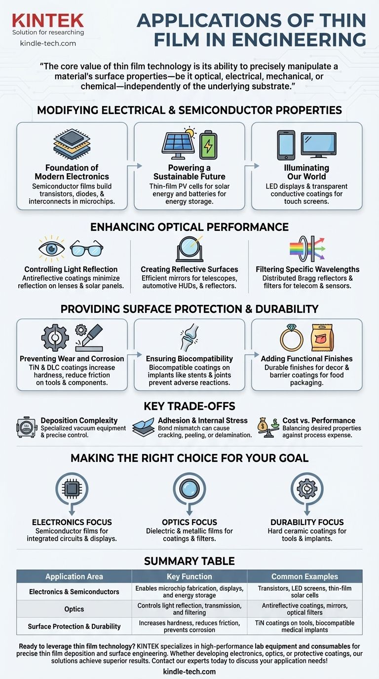
In modern engineering, thin films are a foundational technology used to impart specific, high-performance properties onto the surface of a material. These applications range from creating the complex semiconductor layers that power our electronic devices to applying durable protective coatings that prevent corrosion on tools and aerospace components.
The core value of thin film technology is its ability to precisely manipulate a material's surface properties—be it optical, electrical, mechanical, or chemical—independently of the underlying substrate. This enables the creation of high-performance components that are otherwise impossible to manufacture.
Modifying Electrical and Semiconductor Properties
The most transformative application of thin films is in electronics, where they are used to build devices layer by atomic layer. This is the bedrock of the entire digital revolution.
The Foundation of Modern Electronics
Semiconductor thin films are the active components in virtually all modern electronics. Materials like silicon, gallium arsenide (GaAs), and various nitrides are deposited in precise patterns.
These layers form the transistors, diodes, and interconnects that make up the microchips in computers, mobile phones, and all other smart devices. Emerging research also uses ferromagnetic films to develop new forms of computer memory.
Powering a Sustainable Future
Thin-film photovoltaic cells are a critical part of the solar energy industry. By depositing layers of semiconductor material onto glass or flexible substrates, engineers create efficient and lightweight solar panels.
Similarly, thin-film batteries offer new possibilities for energy storage, enabling more compact and flexible power sources for a range of devices.
Illuminating Our World
The vibrant screens on our phones, televisions, and computers are built using thin films. LED displays and other flat-panel technologies rely on depositing layers of light-emitting or light-modulating materials.
This technology also enables transparent conductive coatings for touch screens, allowing electrical signals to pass through a clear surface.
Enhancing Optical Performance
Thin films provide engineers with precise control over light. By stacking multiple layers with different refractive indices, they can manipulate how light is reflected, transmitted, or filtered.
Controlling Light Reflection
Perhaps the most common optical application is the antireflective coating found on eyeglasses, camera lenses, and solar panels. These incredibly thin layers are engineered to minimize reflection, maximizing light transmission and reducing glare.
Creating Reflective Surfaces
Conversely, thin films are used to create highly efficient mirrors. These are not just for household use but are critical components in reflector lamps, telescopes, and automotive head-up displays (HUDs), where information is projected onto the windshield.
Filtering Specific Wavelengths
Engineers can design complex stacks of thin films, such as distributed Bragg reflectors and narrow-bandpass filters, that selectively reflect or transmit specific colors of light. These are essential in telecommunications, sensors, and scientific instruments.
Providing Surface Protection and Durability
One of the most practical applications of thin films is to make components last longer and perform better under harsh conditions. These coatings provide properties the bulk material lacks.
Preventing Wear and Corrosion
Hard, inert materials like titanium nitride (TiN) and diamond-like carbon (DLC) are applied as thin films to cutting tools, engine components, and industrial equipment.
These protective coatings dramatically increase surface hardness, reduce friction, and provide a barrier against corrosion, extending the life of critical parts in the automotive, aerospace, and defense industries.
Ensuring Biocompatibility
In the medical field, thin films are applied to implants like artificial joints and stents. These coatings can make the device more durable and, more importantly, biocompatible, preventing adverse reactions with the body.
Adding Functional Finishes
Thin films are also used for decorative purposes on items like jewelry or bathroom fittings, providing a durable and attractive finish. Beyond aesthetics, they are used in food packaging to create a barrier that preserves freshness.
Understanding the Key Trade-offs
While powerful, thin film technology is not without its challenges. The process of creating these layers is a highly controlled engineering discipline with critical constraints.
Deposition Complexity
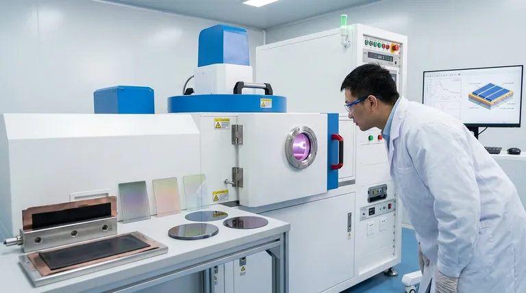
Applying a film that is often only nanometers thick requires specialized vacuum equipment and precise control over temperature, pressure, and source materials. Processes like Physical Vapor Deposition (PVD) are complex and capital-intensive.
Adhesion and Internal Stress
A film is only as good as its bond to the substrate. Ensuring perfect adhesion is a major challenge, as mismatches in material properties can cause internal stress, leading the film to crack, peel, or delaminate.
Cost vs. Performance
The advanced performance enabled by thin films comes at a cost. Engineers must constantly balance the desired surface property against the expense and complexity of the deposition process required to achieve it.
Making the Right Choice for Your Goal
The application of thin film technology is dictated entirely by the specific surface property you need to achieve for your component.
- If your primary focus is electronics and computing: You will leverage semiconductor thin films to build integrated circuits, displays, and memory devices.
- If your primary focus is performance optics: You will use dielectric and metallic films to create antireflective coatings, filters, and specialized mirrors.
- If your primary focus is mechanical durability: You will apply hard ceramic coatings like TiN or DLC to protect tools, engine parts, and medical implants from wear and corrosion.
Ultimately, thin film engineering provides a precise and powerful toolkit for controlling the surface of the physical world.
Summary Table:
| Application Area | Key Function | Common Examples |
|---|---|---|
| Electronics & Semiconductors | Enables microchip fabrication, displays, and energy storage | Transistors, LED screens, thin-film solar cells |
| Optics | Controls light reflection, transmission, and filtering | Antireflective coatings, mirrors, optical filters |
| Surface Protection & Durability | Increases hardness, reduces friction, prevents corrosion | TiN coatings on tools, biocompatible medical implants |
Ready to leverage thin film technology for your engineering challenges? KINTEK specializes in high-performance lab equipment and consumables for precise thin film deposition and surface engineering. Whether you're developing next-generation electronics, advanced optics, or durable protective coatings, our solutions help you achieve superior results. Contact our experts today to discuss how we can support your specific application needs!
Visual Guide
Related Products
- Aluminum-Plastic Flexible Packaging Film for Lithium Battery Packaging
- Thin-Layer Spectral Electrolysis Electrochemical Cell
People Also Ask
- Is there a way to test lithium batteries? Understand Voltage vs. True Health
- What is organic thin film? A Guide to Engineered Molecular Layers for Advanced Tech
- What is the thinnest coating? Unlocking Unique Properties at the Atomic Scale
- What is the difference between single layer film and multi layer film? A Guide to Material Selection
- What are the properties of Aluminium (Al) relevant to its use in coatings? High Reflectivity & Conductivity Explored

