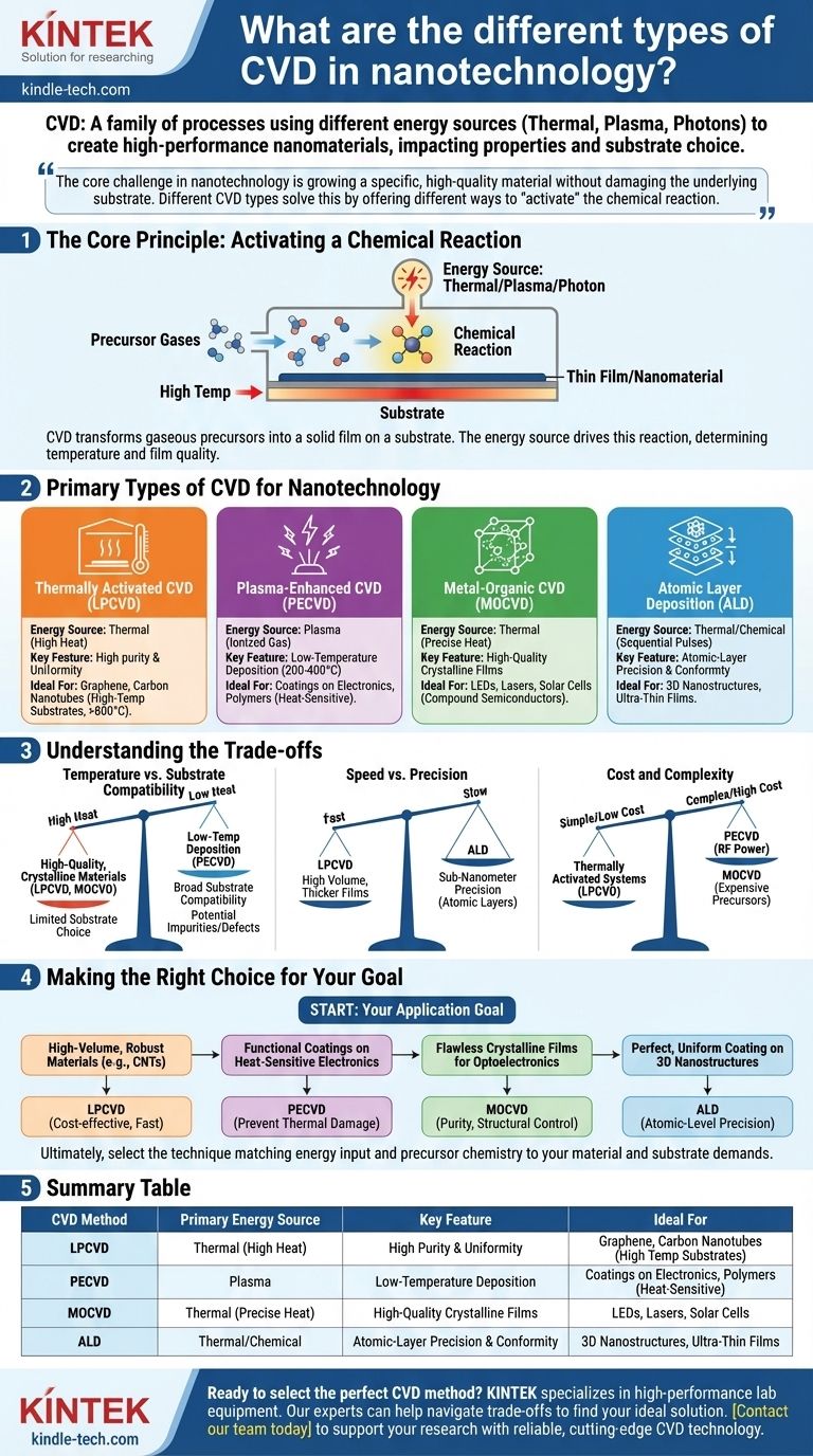
Chemical Vapor Deposition (CVD) is not a single technique but a family of powerful processes used to create high-performance nanomaterials. These methods are primarily distinguished by the type of energy used to initiate the chemical reaction that forms the material, such as thermal energy (heat), plasma, or photons (light). This distinction is critical in nanotechnology, as the choice of method directly dictates the properties of the resulting material and the types of substrates that can be used.
The core challenge in nanotechnology is growing a specific, high-quality material without damaging the underlying substrate. The different types of CVD exist to solve this problem by offering different ways to "activate" the chemical reaction—some use high heat for purity, while others use plasma to enable growth at much lower, safer temperatures.
The Core Principle: Activating a Chemical Reaction
All CVD processes share a fundamental goal: to transform gaseous precursor molecules into a solid thin film or nanomaterial on a substrate. The classification of CVD methods comes from how this transformation is energized.
How CVD Works
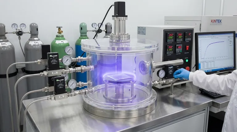
In any CVD process, volatile precursor gases are introduced into a reaction chamber containing a substrate. These gases interact on or near the heated substrate surface, causing them to decompose and react. This chemical reaction results in the deposition of a solid, nonvolatile material onto the substrate.
The Role of the Energy Source
The key differentiator between CVD types is the energy source used to drive the reaction. The choice of energy determines the processing temperature, the quality of the deposited film, and the compatibility with different substrate materials. Traditional methods rely on high heat, but modern techniques have been developed to overcome this limitation.
Primary Types of CVD for Nanotechnology
For nanotechnology applications, the most critical CVD variants are those that offer precise control over material growth, purity, and structure at potentially lower temperatures.
Thermally Activated CVD (APCVD & LPCVD)
This is the most conventional form of CVD, relying purely on thermal energy from a heated substrate to initiate the reaction. It is often subdivided by pressure: Atmospheric Pressure CVD (APCVD) and Low-Pressure CVD (LPCVD). LPCVD is common in nanotechnology for producing higher-purity films with better uniformity.
This method is a workhorse for producing robust materials like graphene and carbon nanotubes (CNTs), which can withstand the high temperatures required (often >800°C).
Plasma-Enhanced CVD (PECVD)
PECVD utilizes an electric field to generate a plasma (an ionized gas) within the reaction chamber. This highly energetic plasma provides the energy to break down precursor gases, allowing deposition to occur at significantly lower temperatures (typically 200-400°C).
This technique is essential for depositing films on temperature-sensitive substrates, such as plastics, polymers, or electronic devices that would be damaged by the heat of traditional CVD.
Metal-Organic CVD (MOCVD)
MOCVD is a specialized form of thermal CVD that uses metal-organic compounds as precursors. These precursors are highly pure and decompose cleanly, making MOCVD the premier technique for growing high-quality single-crystal thin films.
It is the industry standard for manufacturing compound semiconductors used in high-performance LEDs, lasers, and solar cells, where crystalline perfection is paramount.
Atomic Layer Deposition (ALD)
While technically a distinct process, ALD is often considered an advanced subtype of CVD. It involves a sequential, self-limiting process where precursor gases are introduced one at a time. Each pulse deposits exactly one atomic layer of material.
ALD offers unparalleled precision, conformity, and thickness control, making it ideal for coating complex, three-dimensional nanostructures or creating ultra-thin gate oxides in advanced microelectronics.
Understanding the Trade-offs
Choosing a CVD method involves balancing competing factors. Your decision will directly impact the cost, speed, and final quality of your nanomaterial.
Temperature vs. Substrate Compatibility
High temperatures used in LPCVD or MOCVD often lead to higher-quality, more crystalline materials. However, this heat severely limits the choice of substrates. PECVD solves this by enabling low-temperature deposition, but the plasma environment can sometimes introduce impurities or structural defects.
Speed vs. Precision
Standard CVD methods like LPCVD can deposit material relatively quickly, making them suitable for thicker films or large-scale production. In contrast, ALD provides ultimate, sub-nanometer precision but is exceptionally slow, as it builds the material one atomic layer at a time.
Cost and Complexity
Thermally activated systems are often the simplest and most cost-effective to build and operate. PECVD systems require expensive radio-frequency (RF) power supplies to generate the plasma, while MOCVD relies on highly pure and often costly metal-organic precursors, increasing operational expenses.
Making the Right Choice for Your Goal
The optimal CVD technique is determined entirely by your application's specific requirements for material quality, substrate type, and production scale.
- If your primary focus is high-volume production of robust materials like carbon nanotubes: LPCVD offers a cost-effective and reliable solution due to its relative simplicity and speed.
- If your primary focus is depositing functional coatings on heat-sensitive electronics or polymers: PECVD is the necessary choice to prevent thermal damage to the underlying substrate.
- If your primary focus is creating flawless crystalline films for high-performance optoelectronics: MOCVD provides the purity and structural control required for devices like LEDs and lasers.
- If your primary focus is achieving perfect, uniform coating on complex 3D nanostructures: ALD is the only technique that offers the required atomic-level precision and conformity.
Ultimately, selecting the right CVD technique is about matching the energy input and precursor chemistry to the specific demands of your material and substrate.
Summary Table:
| CVD Method | Primary Energy Source | Key Feature | Ideal For |
|---|---|---|---|
| LPCVD | Thermal (High Heat) | High Purity & Uniformity | Graphene, Carbon Nanotubes (High Temp Substrates) |
| PECVD | Plasma | Low-Temperature Deposition | Coatings on Electronics, Polymers (Heat-Sensitive) |
| MOCVD | Thermal (Precise Heat) | High-Quality Crystalline Films | LEDs, Lasers, Solar Cells |
| ALD | Thermal/Chemical | Atomic-Layer Precision & Conformity | 3D Nanostructures, Ultra-Thin Films |
Ready to select the perfect CVD method for your nanotechnology project? The right equipment is critical for achieving the desired material properties and substrate compatibility. KINTEK specializes in providing high-performance lab equipment and consumables tailored to your laboratory's unique needs. Our experts can help you navigate the trade-offs between temperature, speed, and precision to find the ideal solution.
Contact our team today to discuss how we can support your research and development with reliable, cutting-edge CVD technology.
Visual Guide
Related Products
- CVD Diamond Dressing Tools for Precision Applications
- Multi Heating Zones CVD Tube Furnace Machine Chemical Vapor Deposition Chamber System Equipment
- CVD Diamond Domes for Industrial and Scientific Applications
- CVD Diamond for Thermal Management Applications
- Chemical Vapor Deposition CVD Equipment System Chamber Slide PECVD Tube Furnace with Liquid Gasifier PECVD Machine
People Also Ask
- What are the disadvantages of CVD diamonds? Understanding the trade-offs for your purchase.
- What is CVD diamond? The Ultimate Guide to Lab-Grown Diamonds and Their Uses
- How long does it take to make synthetic diamonds? Discover the 6-8 Week Science Behind Lab-Grown Gems
- What color diamonds are CVD? Understanding the Process from Brown Tint to Colorless Beauty
- Can CVD diamonds change color? No, their color is permanent and stable.


