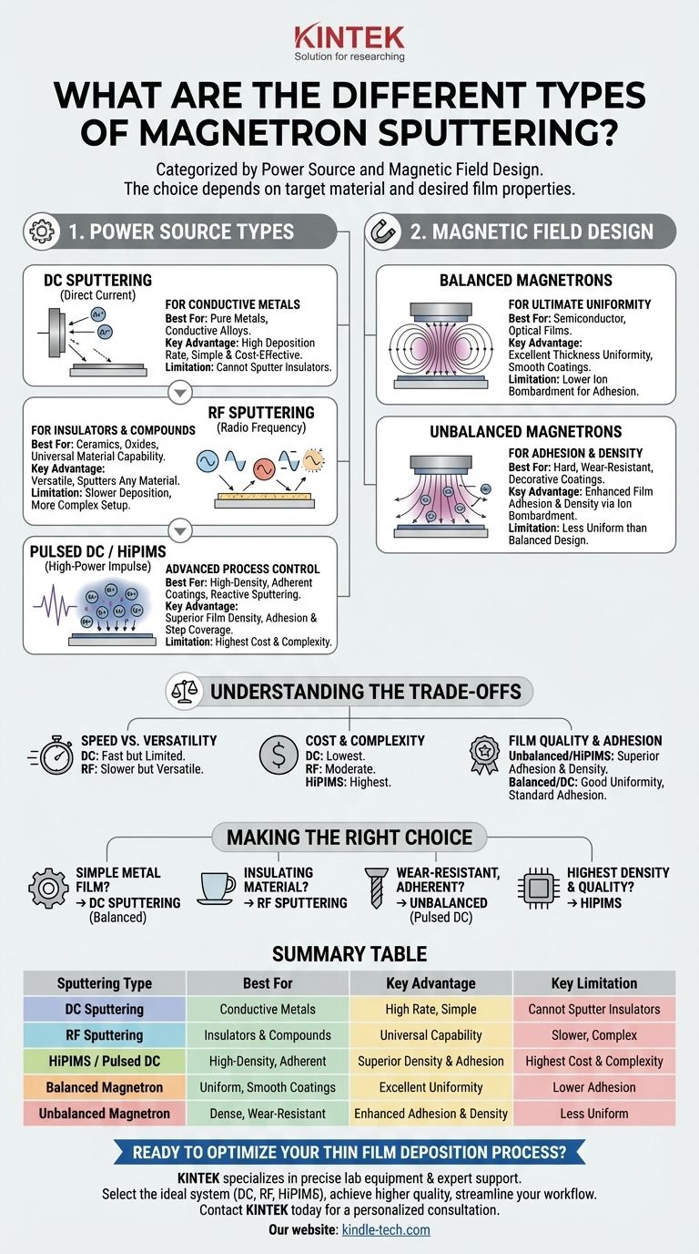
At its core, magnetron sputtering is categorized by two key factors: the type of electrical power used to generate the plasma and the design of the magnetic field that confines it. The primary power source types are Direct Current (DC), Radio Frequency (RF), and advanced pulsed systems like HiPIMS. These choices are determined by the electrical properties of the material you intend to deposit.
The fundamental decision between sputtering types comes down to your target material and desired film quality. For conductive metals, DC is the standard. For insulators and compounds, RF is necessary. For the highest density and adhesion, advanced pulsed techniques are used.
The Core Distinction: Power Source and Material Type
The most significant differentiator between sputtering techniques is the power supply. This choice is not arbitrary; it is dictated by the electrical conductivity of the target material you want to deposit as a thin film.
DC Sputtering: The Workhorse for Conductors
Direct Current (DC) sputtering is the simplest and most common form. It applies a constant negative voltage to the target material.
This steady voltage attracts positive ions (typically argon) from the plasma, which strike the target and eject atoms. This process is efficient and fast, but it has a critical limitation.
It only works for electrically conductive targets, like pure metals and some conductive alloys.
RF Sputtering: The Solution for Insulators
Radio Frequency (RF) sputtering uses a high-frequency alternating voltage instead of a constant DC voltage.
This rapid switching of polarity prevents the buildup of positive charge on the surface of electrically insulating materials (like ceramics or oxides), which would otherwise halt the sputtering process.
While slightly more complex and often slower than DC, RF sputtering's key advantage is its versatility—it can deposit a film from virtually any material, conductor or insulator.
Pulsed DC and HiPIMS: Advanced Process Control
Pulsed DC is an evolution of standard DC sputtering. Instead of a constant voltage, it applies power in short, high-energy pulses. This is particularly useful in reactive sputtering, where a gas like oxygen or nitrogen is introduced to form a compound film (e.g., a metal oxide or nitride).
HiPIMS (High-Power Impulse Magnetron Sputtering) takes this concept to an extreme, delivering very high power in extremely short pulses. This creates a highly dense plasma with a large fraction of ionized target material.
The result is films with exceptional density, superior adhesion, and excellent coverage on complex shapes, making it a state-of-the-art technique for high-performance applications.
A Second Factor: Magnetic Field Design
Beyond the power source, the physical design of the magnetron's magnetic field also defines the sputtering process and the resulting film properties.
Balanced Magnetrons: For Ultimate Uniformity
In a balanced magnetron, the magnetic field lines are configured to tightly confine the plasma directly in front of the target.
This maximizes the ionization efficiency near the target, leading to a stable process that produces very uniform and smooth coatings. This is the preferred configuration for applications like semiconductor and optical films where consistent thickness is critical.
Unbalanced Magnetrons: For Adhesion and Density
In an unbalanced magnetron, some of the magnetic field lines are intentionally directed away from the target and toward the substrate.
This design guides a portion of the plasma ions to the substrate, resulting in a low-energy ion bombardment of the film as it grows. This bombardment creates denser films with significantly stronger adhesion, making it ideal for hard or wear-resistant decorative coatings.
Understanding the Trade-offs
Choosing the right sputtering technique involves balancing performance, complexity, and cost. Each method has clear advantages and disadvantages.
Speed vs. Material Versatility
DC sputtering offers the highest deposition rates and is the most straightforward process, but it is strictly limited to conductive materials.
RF sputtering provides near-universal material capability but is generally slower and requires more complex hardware (like an impedance matching network) to operate efficiently.
Cost and Complexity
The equipment hierarchy follows a clear path. DC systems are the simplest and most cost-effective. RF systems are moderately more complex and expensive.
HiPIMS represents the peak in both performance and complexity, requiring specialized power supplies and process control, making it the most significant investment.
Film Quality and Adhesion
Standard DC sputtering produces high-quality metallic films suitable for most applications. However, for the most demanding requirements, other methods excel.
Unbalanced magnetrons provide a clear advantage in film adhesion and density over balanced systems. HiPIMS delivers the highest possible film quality, achieving densities that are nearly impossible with other techniques.
Making the Right Choice for Your Application
Your choice of magnetron sputtering technique should be driven directly by your material requirements and performance goals.
- If your primary focus is depositing a simple metal film efficiently: DC sputtering with a balanced magnetron is the most direct and cost-effective solution.
- If your primary focus is depositing an insulating material like a ceramic or oxide: RF sputtering is the essential and required technology for the job.
- If your primary focus is a dense, wear-resistant coating with maximum adhesion: Unbalanced magnetron sputtering, often using pulsed DC in a reactive process, is the ideal choice.
- If your primary focus is achieving the highest possible film density and quality for a critical application: HiPIMS is the state-of-the-art method that provides unparalleled results.
By matching the sputtering technique to your specific material and performance targets, you gain precise control over the properties of your thin film.
Summary Table:
| Sputtering Type | Best For | Key Advantage | Key Limitation |
|---|---|---|---|
| DC Sputtering | Conductive Metals (e.g., Au, Ag, Al) | High Deposition Rate, Simple & Cost-Effective | Cannot Sputter Insulating Materials |
| RF Sputtering | Insulators & Compounds (e.g., Al2O3, SiO2) | Universal Material Capability | Slower Deposition, More Complex Setup |
| HiPIMS / Pulsed DC | High-Density, Adherent Coatings | Superior Film Density & Step Coverage | Highest Cost & Process Complexity |
| Balanced Magnetron | Uniform, Smooth Coatings (e.g., Optical Films) | Excellent Thickness Uniformity | Lower Ion Bombardment for Adhesion |
| Unbalanced Magnetron | Dense, Wear-Resistant Coatings | Enhanced Film Adhesion & Density | Less Uniform than Balanced Design |
Ready to Optimize Your Thin Film Deposition Process?
Choosing the right sputtering technique is critical to achieving your desired film properties, whether you need high uniformity, superior adhesion, or the ability to coat non-conductive materials. KINTEK specializes in providing the precise lab equipment and expert support you need to succeed.
We help you:
- Select the ideal system (DC, RF, HiPIMS) for your specific materials and application goals.
- Achieve higher quality results with reliable, high-performance sputtering equipment and consumables.
- Streamline your workflow with solutions tailored to laboratory research and development needs.
Let's discuss your project. Our experts are ready to help you identify the perfect sputtering solution to enhance your research and development.
Contact KINTEK today for a personalized consultation
Visual Guide
Related Products
- Microwave Plasma Chemical Vapor Deposition MPCVD Machine System Reactor for Lab and Diamond Growth
- Chemical Vapor Deposition CVD Equipment System Chamber Slide PECVD Tube Furnace with Liquid Gasifier PECVD Machine
- Molybdenum Tungsten Tantalum Special Shape Evaporation Boat
- Inclined Rotary Plasma Enhanced Chemical Vapor Deposition PECVD Equipment Tube Furnace Machine
- Inclined Rotary Plasma Enhanced Chemical Vapor Deposition PECVD Equipment Tube Furnace Machine
People Also Ask
- How is a diamond formed from CVD? The Science of Growing Diamonds Atom by Atom
- What are the primary advantages of the CVD method for growing diamonds? Engineering High-Purity Gems and Components
- What is microwave plasma chemical vapor deposition? A Guide to High-Purity Diamond Film Growth
- How do vacuum pumps and valves collaborate in MPCVD? Achieve Precise Pressure Control for Superior CNT Synthesis
- What are the advantages of a Microwave Plasma CVD reactor for MCD/NCD coatings? Precision Multilayer Diamond Engineering