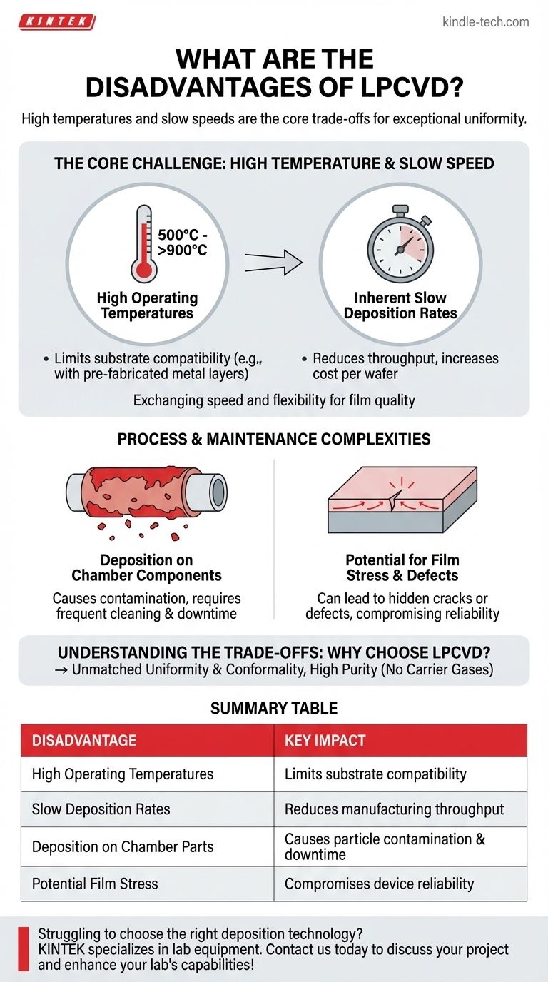
The primary disadvantages of Low-Pressure Chemical Vapor Deposition (LPCVD) are its high operating temperatures, which limit substrate compatibility, and its inherently slow deposition rates, which reduce manufacturing throughput. These are compounded by process challenges like unwanted deposition on chamber components and potential for film stress.
While often considered a workhorse for high-quality thin films, LPCVD's disadvantages are not flaws but fundamental trade-offs. You are essentially exchanging processing speed and flexibility for exceptional film uniformity, purity, and the ability to coat complex topographies.
The Core Challenge: High Temperature and Slow Speed
The defining characteristics of the LPCVD process—low pressure and high heat—are the source of both its greatest strengths and its most significant drawbacks.
The Impact of High Temperatures
LPCVD processes typically operate at high temperatures, often in the range of 500°C to over 900°C. This high thermal budget creates a critical limitation.
It makes the process unsuitable for depositing films on substrates that cannot withstand such heat, such as those with previously fabricated metal layers (like aluminum) or temperature-sensitive materials.
Inherent Slow Deposition Rates
The low-pressure environment, while excellent for uniformity, contributes to a slower reaction rate compared to atmospheric pressure methods.
This directly impacts manufacturing throughput. For applications requiring thick films or high-volume production, the slow speed of LPCVD can become a significant bottleneck and increase the cost per wafer.
Process and Maintenance Complexities
Beyond the core operational characteristics, the practical implementation of LPCVD introduces further challenges that must be managed.
Deposition on Chamber Components
The chemical vapor precursors in an LPCVD system are not selective; they will deposit a film on any surface that is hot enough.
This leads to significant coating of the quartz furnace tube and other internal parts. This unwanted deposition can flake off, creating particle contamination that reduces yield, and necessitates frequent, time-consuming cleaning cycles, leading to equipment downtime.
Potential for Film Stress and Defects
The high temperatures involved in deposition and the subsequent cooling cycle can induce significant thermal stress between the newly deposited film and the underlying substrate.
If not properly managed, this stress can lead to the formation of "hidden cracks" or other film defects, compromising the integrity and reliability of the device.
Challenges with In-Situ Doping
While doping the film during the deposition process (in-situ) is possible, it can be difficult to control. Achieving uniform dopant concentration throughout the film and across the wafer batch can be more complex in an LPCVD system compared to post-deposition methods like ion implantation.
Understanding the Trade-offs: Why Choose LPCVD?
To fully grasp the disadvantages, one must weigh them against the unique advantages that make LPCVD a critical process in semiconductor manufacturing.
The Goal: Unmatched Uniformity and Conformality
LPCVD excels at producing films with outstanding thickness uniformity and conformality (the ability to evenly coat complex, three-dimensional structures like trenches).
The low pressure increases the mean free path of gas molecules, allowing them to reach and coat all surfaces of a complex topography before reacting. This is the primary reason LPCVD is chosen for critical layers like polysilicon gates and silicon nitride passivation.
The Purity Advantage
The process does not require carrier gases, and the low-pressure environment allows reaction by-products to be removed efficiently. This results in films with very high purity and low particle contamination, which is essential for high-performance electronic devices.
Context vs. Other Methods
Every deposition method has its own set of compromises. For example, while Metal-Organic CVD (MOCVD) can be used for different materials, its precursors are often extremely expensive, toxic, and hazardous. LPCVD, despite its drawbacks, is a mature and relatively well-understood process.
Making the Right Choice for Your Application
Selecting a deposition technique requires aligning the process capabilities with your primary engineering goal.
- If your primary focus is exceptional film quality and conformality: LPCVD is often the best choice, provided your substrate can tolerate the high temperatures and your production model can accommodate the slower speed.
- If your primary focus is high throughput on temperature-sensitive substrates: You should explore alternatives like Plasma-Enhanced CVD (PECVD), which operates at much lower temperatures and higher deposition rates.
- If your primary focus is atomic-level precision and control: Consider Atomic Layer Deposition (ALD), which offers unparalleled conformality and thickness control, albeit at even slower speeds than LPCVD.
Understanding these inherent limitations allows you to leverage LPCVD for its unparalleled strengths in the precise applications where quality and uniformity are non-negotiable.
Summary Table:
| Disadvantage | Key Impact |
|---|---|
| High Operating Temperatures | Limits substrate compatibility (e.g., with pre-fabricated metal layers) |
| Slow Deposition Rates | Reduces manufacturing throughput, increases cost per wafer |
| Deposition on Chamber Parts | Causes particle contamination, requires frequent cleaning and downtime |
| Potential Film Stress | Can lead to hidden cracks or defects, compromising device reliability |
Struggling to choose the right deposition technology for your specific application? KINTEK specializes in lab equipment and consumables, serving laboratory needs. Our experts can help you navigate the trade-offs between LPCVD, PECVD, and ALD to find the optimal solution for your film quality, throughput, and substrate requirements. Contact us today to discuss your project and enhance your lab's capabilities!
Visual Guide
Related Products
- Microwave Plasma Chemical Vapor Deposition MPCVD Machine System Reactor for Lab and Diamond Growth
- Chemical Vapor Deposition CVD Equipment System Chamber Slide PECVD Tube Furnace with Liquid Gasifier PECVD Machine
- Customer Made Versatile CVD Tube Furnace Chemical Vapor Deposition Chamber System Equipment
- 915MHz MPCVD Diamond Machine Microwave Plasma Chemical Vapor Deposition System Reactor
- RF PECVD System Radio Frequency Plasma-Enhanced Chemical Vapor Deposition RF PECVD
People Also Ask
- What is microwave plasma chemical vapor deposition? A Guide to High-Purity Diamond Film Growth
- How is a diamond formed from CVD? The Science of Growing Diamonds Atom by Atom
- What are the advantages of a Microwave Plasma CVD reactor for MCD/NCD coatings? Precision Multilayer Diamond Engineering
- How are CVD diamonds created? Discover the Science of Lab-Grown Diamond Precision
- What pressure is needed for chemical vapor deposition of diamonds? Master the Low-Pressure 'Sweet Spot'