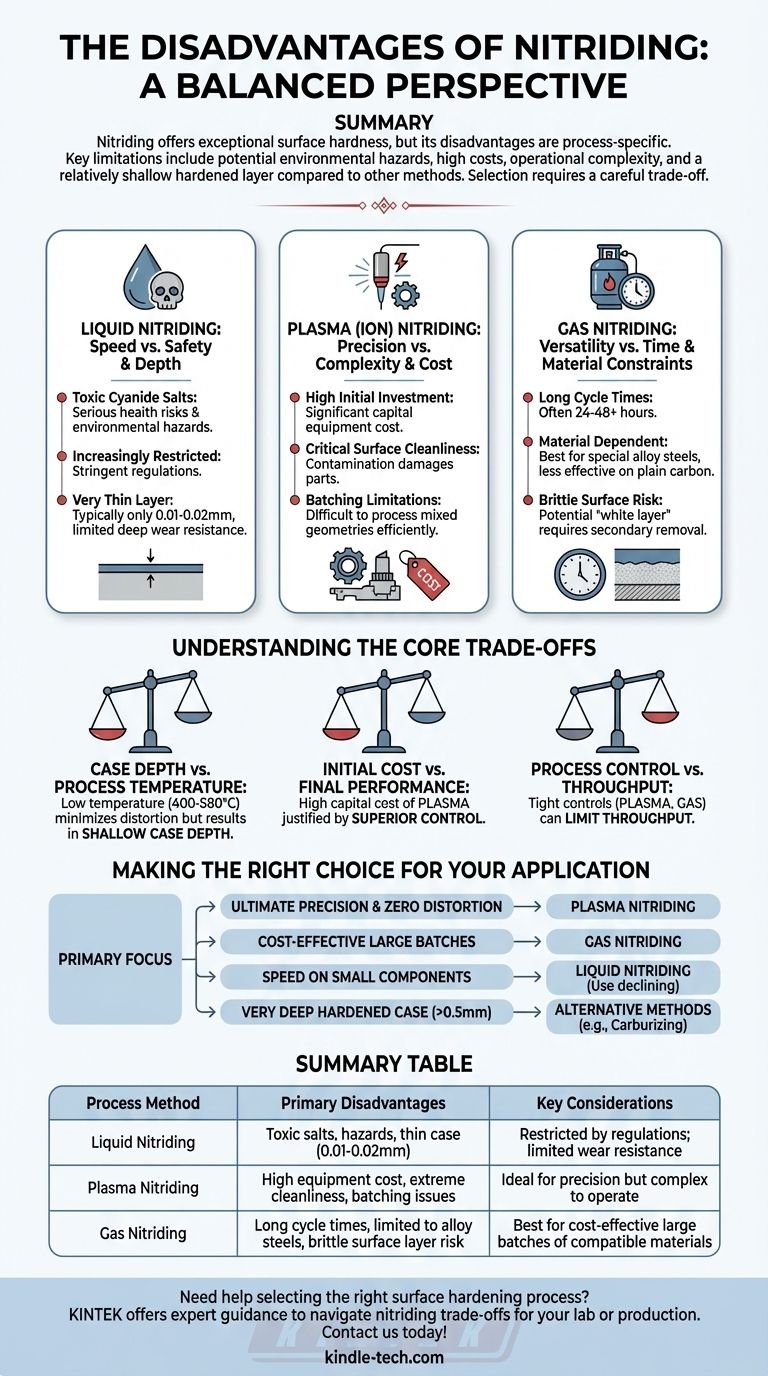
In short, the primary disadvantages of nitriding are its process-specific limitations, including potential environmental hazards with liquid nitriding, high initial costs and operational complexity with plasma nitriding, and the creation of a relatively thin hardened layer compared to other case-hardening methods. These drawbacks mean the selection of a nitriding process requires a careful trade-off between cost, performance requirements, and operational constraints.
While nitriding offers exceptional surface hardness and wear resistance with minimal part distortion, its effectiveness is not universal. The disadvantages are highly dependent on the specific method chosen—liquid, gas, or plasma—and must be weighed against your project's specific material, budget, and performance goals.
Process-Specific Drawbacks: Not All Nitriding is Equal
The term "nitriding" covers several distinct industrial processes. The disadvantages are rarely general and are most often tied to the specific method you are evaluating.
Liquid Nitriding: Speed vs. Safety and Depth
Liquid nitriding is known for its speed but comes with significant compromises. The primary drawback is the use of toxic cyanide salts in many traditional formulations.
This creates serious health risks for operators and significant environmental challenges for waste disposal. Due to these concerns, the process is increasingly restricted by regulations, even with the development of non-toxic alternatives.
Furthermore, liquid nitriding typically produces a very thin hardened layer, often only 0.01-0.02mm, which may not be sufficient for applications requiring deeper wear resistance.
Plasma (Ion) Nitriding: Precision vs. Complexity and Cost
Plasma nitriding offers excellent control but introduces technical and financial hurdles. The most significant is the high initial investment in plasma equipment, which can be a barrier for many operations.
The process itself is also demanding. The cleanliness of the component surface is absolutely critical; any contamination can lead to unstable electrical arcs that can damage the part.
Operationally, there are limitations on batching. Because of the physics of the power-to-surface-area relationship, it is difficult to process components of different sizes or geometries in a single batch, reducing throughput efficiency.
Gas Nitriding: Versatility vs. Time and Material Constraints
Gas nitriding is a widely used method, but it is not without its own set of challenges. Its most notable disadvantage is the long cycle time, which can often extend to 24-48 hours or more, making it slower than other methods.
This process is also dependent on the material being treated. It works best on special alloy steels containing nitride-forming elements like aluminum, chromium, and molybdenum. It is far less effective on plain carbon steels.
If the process parameters are not precisely controlled, gas nitriding can also produce a brittle "white layer" on the surface that may need to be removed through secondary grinding or lapping operations.
Understanding the Core Trade-offs
Choosing a surface hardening process requires acknowledging its inherent limitations. For nitriding, the key trade-offs revolve around depth, cost, and operational realities.
Case Depth vs. Process Temperature
Nitriding is a low-temperature process (typically 400-580°C), which is its greatest advantage as it minimizes distortion. However, this low temperature also limits the diffusion rate of nitrogen, resulting in a relatively shallow case depth compared to higher-temperature processes like carburizing.
Initial Cost vs. Final Performance
The high capital cost of plasma nitriding systems must be justified by the need for superior control over case properties and the ability to treat complex shapes without distortion. For simpler parts where some distortion is tolerable, less expensive methods may be more economical.
Process Control vs. Throughput
The tight controls required for plasma nitriding (cleanliness, batching) and gas nitriding (atmosphere control) can limit throughput. This contrasts with the faster, but more hazardous and less precise, nature of liquid nitriding.
Making the Right Choice for Your Application
Selecting the correct nitriding method, or choosing an alternative, depends entirely on your primary objective.
- If your primary focus is ultimate precision on complex parts with zero distortion: Plasma nitriding is the superior choice, provided you can justify the high initial cost and manage its operational complexities.
- If your primary focus is cost-effective treatment for large batches of suitable alloy steels: Gas nitriding is often the most balanced option, assuming your production schedule can accommodate its longer cycle times.
- If your primary focus is speed on small components and you operate under strict environmental controls: Liquid nitriding could be considered, but its use is declining due to significant health and safety concerns.
- If your primary focus is achieving a very deep hardened case (>0.5mm): You should evaluate alternative case-hardening processes like carburizing, as nitriding is fundamentally a shallow-case method.
Understanding these limitations is the first step toward leveraging nitriding's powerful advantages effectively.
Summary Table:
| Process Method | Primary Disadvantages | Key Considerations |
|---|---|---|
| Liquid Nitriding | Toxic cyanide salts, environmental hazards, very thin case depth (0.01-0.02mm) | Increasingly restricted by regulations; limited wear resistance |
| Plasma Nitriding | High initial equipment cost, requires extreme surface cleanliness, difficult batch processing | Ideal for precision but complex to operate |
| Gas Nitriding | Long cycle times (24-48+ hours), limited to specific alloy steels, risk of brittle surface layer | Best for cost-effective large batches of compatible materials |
Need help selecting the right surface hardening process for your lab or production needs? KINTEK specializes in lab equipment and consumables, offering expert guidance to help you navigate the trade-offs of nitriding and other methods. Whether you're dealing with material constraints, budget considerations, or performance requirements, we provide tailored solutions to enhance your operational efficiency. Contact us today to discuss your project and discover how KINTEK can support your laboratory goals!
Visual Guide