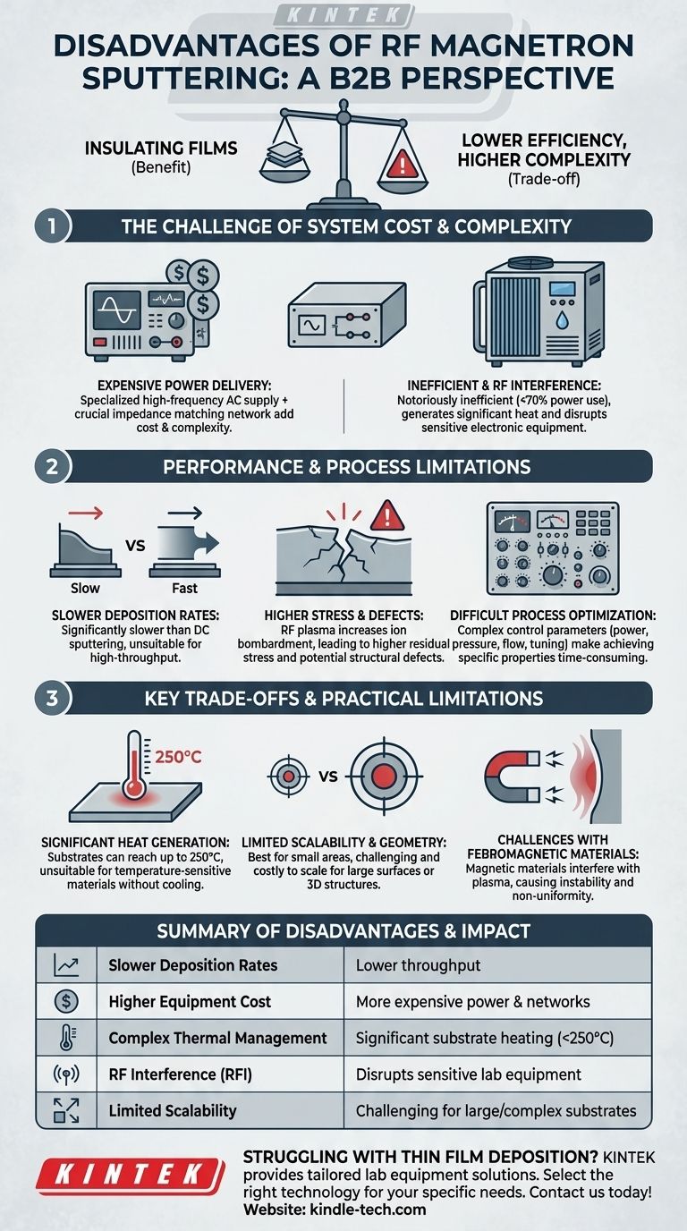
While essential for depositing insulating materials, RF magnetron sputtering is not a universally superior technique. Its primary disadvantages are significantly slower deposition rates compared to DC sputtering, higher equipment cost and system complexity, and substantial challenges related to thermal management and process control. These factors often limit its use to smaller-scale or specialized applications where depositing dielectrics is the main objective.
The core trade-off of RF sputtering is accepting lower efficiency and higher complexity in exchange for the unique ability to deposit insulating and dielectric thin films. Understanding this trade-off is critical for determining if its disadvantages outweigh its benefits for your specific application.
The Challenge of System Cost and Complexity
The primary barrier to adopting RF sputtering is often economic and operational. The equipment required is inherently more complex and expensive than its DC counterpart.
The Expensive Power Delivery System
An RF system requires a specialized, high-frequency AC power supply, which is significantly more expensive than a standard DC power supply.
Furthermore, it mandates an impedance matching network between the power supply and the sputtering chamber. This device is crucial for efficiently transferring power to the plasma but adds another layer of cost, complexity, and potential failure.
Inefficient Power and RF Interference
RF power supplies are notoriously inefficient, often converting less than 70% of input power into usable RF energy. The rest is lost as heat, necessitating robust cooling systems (often water-cooling for units over 1 kW) and increasing operational energy costs.
These systems also generate significant radio-frequency interference (RFI). This electronic "noise" can disrupt other sensitive equipment, requiring careful shielding and mitigation strategies, which adds to the system's overall complexity.
Performance and Process Limitations
Beyond the hardware, RF sputtering presents several performance-related challenges that can impact the quality of the final film and the efficiency of the process.
Slower Deposition Rates
A near-universal disadvantage of RF sputtering is its slower deposition rate compared to DC magnetron sputtering for conductive materials. This makes it less suitable for applications requiring high-throughput production or the creation of very thick films.
Higher Residual Stress and Defects
The nature of the RF plasma can lead to higher ion bombardment on the substrate. While this can sometimes improve film density, it often results in higher internal residual stress, especially in thicker coatings.
This increased bombardment can also introduce more structural defects into the film, potentially compromising its electrical or mechanical properties.
Difficult Process Optimization
Optimizing an RF sputtering process can be a time-consuming endeavor. The large number of control parameters—including power, pressure, gas flow, and the tuning of the impedance matching network—creates a complex landscape to navigate when trying to achieve specific film properties.
Understanding the Key Trade-offs
The decision to use RF sputtering involves balancing its unique capability against several practical limitations, particularly concerning heat and scale.
Significant Heat Generation
A large portion of the energy delivered to the target in an RF system is converted directly into heat. This requires an efficient cooling system for the target to prevent overheating and damage.
Simultaneously, the substrate is subjected to significant heating from the plasma, with temperatures potentially reaching 250°C. This makes RF sputtering unsuitable for depositing films on temperature-sensitive substrates without advanced cooling solutions.
Limitations on Substrate Size and Geometry
RF sputtering is most effective and commonly used for smaller substrate areas. Scaling the process for uniform deposition over large surfaces is technically challenging and expensive.
It also struggles to deposit uniform coatings on substrates with complex, three-dimensional structures, as the plasma distribution can be non-uniform.
Challenges with Ferromagnetic Materials
When sputtering magnetic materials like iron or nickel, the material's own magnetic field can interfere with and disturb the plasma. This can lead to an unstable process and non-uniform deposition.
Making the Right Choice for Your Application
Selecting the correct sputtering method requires aligning the technique's strengths and weaknesses with your primary goal.
- If your primary focus is depositing high-quality insulating films in a research setting: RF sputtering is the correct tool, but you must budget for the complex power system and manage substrate heating.
- If your primary focus is high-speed, large-area industrial production of conductive films: The slow rates and scalability issues of RF sputtering make DC or pulsed-DC magnetron sputtering a far more economical choice.
- If your primary focus is depositing films onto temperature-sensitive substrates: Be aware that RF sputtering introduces significant heat, and you will need to invest in or design a robust substrate cooling solution to prevent damage.
Understanding these inherent trade-offs is the first step toward selecting the right deposition technology for your specific technical and economic goals.
Summary Table:
| Disadvantage | Key Impact |
|---|---|
| Slower Deposition Rates | Lower throughput compared to DC sputtering |
| Higher Equipment Cost | More expensive power supplies and matching networks |
| Complex Thermal Management | Significant substrate heating (up to 250°C) |
| RF Interference (RFI) | Can disrupt sensitive lab equipment |
| Limited Scalability | Challenging for large-area or complex substrates |
Struggling with thin film deposition challenges? KINTEK specializes in lab equipment and consumables, providing tailored solutions for your laboratory needs. Whether you're depositing insulating films or require high-throughput conductive coatings, our experts can help you select the right sputtering technology. Contact us today to optimize your process and achieve superior results!
Visual Guide
Related Products
- RF PECVD System Radio Frequency Plasma-Enhanced Chemical Vapor Deposition RF PECVD
- Spark Plasma Sintering Furnace SPS Furnace
People Also Ask
- What is plasma enhanced chemical vapour deposition PECVD used for? Enable Low-Temp Thin Films for Electronics & Solar
- How does plasma enhance CVD? Unlock Low-Temperature, High-Quality Film Deposition
- What is plasma enhanced chemical Vapour deposition process used for fabrication of? A Guide to Low-Temperature Thin Films
- What is plasma chemical vapor deposition? A Low-Temperature Thin Film Coating Solution
- Why is a Matching Network Indispensable in RF-PECVD for Siloxane Films? Ensure Stable Plasma and Uniform Deposition

